In today's rapidly evolving electronics landscape, the demand for advanced PCB technologies is at an all-time high. With the global PCB market projected to reach $82.98 billion by 2026 as reported by MarketsandMarkets, it is clear that innovation in this field is essential for competitive advantage. Advanced PCBs are not only enhancing the performance and reliability of electronic devices but are also enabling the miniaturization of components, which is crucial for modern applications ranging from consumer electronics to automotive and industrial systems.
Dr. Helen Zhang, a leading expert in PCB technology and author of several industry reports, highlights the importance of these innovations: "The shift towards advanced PCBs is not just a trend; it's a necessity for meeting the increasing complexities of electronic design." With advancements such as multilayering, embedded components, and flexible circuit technologies, designers are now able to push the boundaries of what's possible in electronics. These technologies are transforming how products are conceived and manufactured, ultimately leading to smarter, faster, and more efficient devices.
As we delve into the top 10 advanced PCB technologies reshaping the industry, it becomes evident that understanding and implementing these innovations will be vital for engineers and companies looking to stay ahead in a competitive market. The future of electronics design is here, and it hinges on the capabilities offered by advanced PCBs.

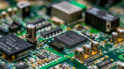
The evolution of printed circuit board (PCB) technologies is dramatically reshaping the landscape of electronics design, ushering in innovative solutions that cater to the increasingly complex demands of modern devices. Advanced PCB technologies, such as multi-layer designs, high-frequency materials, and embedded component integration, are crucial in enhancing circuit density and performance. As devices become smaller and more powerful, these technologies enable engineers to create circuitry that optimizes space while delivering improved electrical characteristics.
Moreover, the integration of advanced manufacturing techniques, such as additive manufacturing and automated assembly, further revolutionizes the way PCBs are produced. These methods not only streamline the production process but also reduce waste and lower costs, making it feasible to develop more intricate and functional designs. This transformation impacts not just consumer electronics, but also critical sectors like medical devices and aerospace, where reliability and efficiency are paramount. As such, the continuous innovation in PCB technologies drives the electronics industry towards more compact, robust, and cutting-edge applications that meet the needs of today's dynamic market.
This bar chart represents the prevalence of various advanced PCB technologies in modern electronics design, showcasing their impact on enhancing performance and functionality.
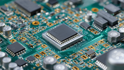
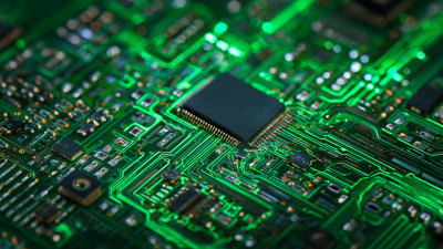
High-density interconnects (HDI) are revolutionizing the landscape of electronics design, facilitating miniaturization and enhancing functionality. As electronic devices become increasingly compact, the demand for more efficient and sophisticated PCBs has surged. HDI technology allows for the integration of smaller features, finer wiring, and improved connectivity, making it possible to fit more functionality into smaller physical spaces. This transformative approach not only saves space but also enhances signal integrity, which is crucial for high-speed applications.
Tips for adopting HDI technology include investing in advanced design software that can accommodate the complexities of HDI layouts. This software can significantly streamline the design process, allowing for precise placement of components and optimized routing paths. Additionally, consider collaboration with manufacturers experienced in HDI fabrication to ensure that your designs are both manufacturable and reliable.
When transitioning to HDI, it is important to meticulously plan your PCB layer stack-up and understand the implications of via types, such as microvias and blind/buried vias. These decisions can affect the performance, cost, and manufacturability of your product. Always conduct thorough simulations and prototyping to validate your designs before moving to full-scale production. By embracing HDI technology, designers can push the limits of innovation while meeting the ever-growing demand for compact and capable electronic devices.
| Technology | Description | Benefits | Applications |
|---|---|---|---|
| High-Density Interconnect (HDI) | A PCB with closely packed circuitry that allows for increased density. | Miniaturization, improved performance, and reduced signal loss. | Mobile devices, medical equipment, and aerospace. |
| Flexible PCBs | A flexible circuit board that can bend and fold. | Lightweight, space-saving, and adaptable designs. | Wearable technology and consumer electronics. |
| Embedded Components | Components integrated directly within the PCB layers. | Reduced assembly costs and improved reliability. | IoT devices and automotive applications. |
| Microwave PCBs | Designed for high-frequency applications. | Enhanced signal integrity at microwave frequencies. | Telecommunications and radar systems. |
| Thermal Management PCBs | PCBs designed to dissipate heat efficiently. | Extended lifespan of components and improved performance. | Power electronics and LED lighting. |
| Rigid-Flex PCBs | Combines rigid and flexible PCB technologies. | Versatility in design and reduced weight. | Consumer electronics and aerospace. |
| 3D Printed PCBs | PCBs created using additive manufacturing techniques. | Rapid prototyping and low-volume production. | Rapid testing and compact devices. |
| Nano-Coating Technologies | Protective coatings at the nanoscale. | Enhances durability and moisture resistance. | Electronics in harsh environments. |
| High-Speed PCB Technologies | Design techniques for improved signal speed. | Lower latency and better data handling. | Networking equipment and high-frequency applications. |

Emerging materials are at the forefront of transforming printed circuit board (PCB) technology, significantly enhancing performance and durability in modern electronics design. A notable advancement is the integration of high-performance polymers and composites, which offer superior thermal stability and dielectric properties. These materials not only improve signal integrity but also enable PCBs to withstand more extreme environmental conditions, making them ideal for applications in automotive, aerospace, and industrial sectors. The shift towards lightweight materials is also pivotal, allowing for the development of more compact devices without compromising functionality.
Additionally, advancements in nanotechnology are yielding innovative materials that augment the electrical characteristics of PCBs. For instance, the use of nanostructured conductive materials provides enhanced conductivity while reducing the overall weight of the boards. These developments lead to increased component density and efficiency, fostering smaller and more powerful electronic devices. Furthermore, the introduction of environmentally friendly materials helps meet sustainability goals within the industry, ensuring that performance improvements do not come at the expense of ecological responsibility. This multifaceted approach to material innovation is critical for the next generation of electronics, pushing the boundaries of what is possible in PCB design.
Flexible and rigid-flex printed circuit boards (PCBs) are at the forefront of modern electronics design, revolutionizing how devices are constructed and function. These advanced technologies enable manufacturers to create intricate and compact device layouts, adapting seamlessly to a range of form factors. Flexible PCBs, which can bend and conform to tight spaces, allow for innovative designs in wearable technology, medical devices, and consumer electronics, making them essential for applications where weight and space are significant considerations.
Rigid-flex PCBs combine the benefits of both rigid and flexible designs, offering enhanced durability and reliability in complex systems. By integrating multiple layers of flexible circuits into a rigid structure, they facilitate connectivity while minimizing the need for connectors and reducing the overall size of the device. This capability is particularly advantageous in industries such as aerospace and automotive, where harsh environments necessitate robust and lightweight solutions. As these PCB technologies continue to evolve, they play a critical role in driving the next generation of electronic devices, enabling greater functionality and efficiency without sacrificing design aesthetics.

The demand for compact and multifunctional electronic devices is pushing the boundaries of PCB (Printed Circuit Board) technology. As designers seek to maximize the functionality of their products while minimizing size, advanced circuit integration trends are emerging. Techniques such as 3D packaging, embedded components, and high-density interconnects are becoming essential in achieving greater design efficiency. By embedding passive components directly into the PCB, designers can free up space for other critical elements, enhancing the overall functionality of the device.
Tips for optimizing PCB designs include utilizing software tools that allow for advanced simulation and analysis. These tools can help identify potential issues early in the design process, reducing the need for costly revisions later. Additionally, consider adopting a modular approach, where various functions can be integrated into separate, but interconnected, components. This not only simplifies the design process but also allows for easier upgrades in the future without reinventing the entire board.
To stay ahead in this rapidly evolving field, keep an eye on emerging technologies such as flexible PCBs and nanomaterials, which promise even tighter integration of circuit functions. Utilizing these innovations can significantly enhance the performance of electronic designs while adhering to space constraints. By embracing these advanced PCB technologies and integration strategies, designers can create cutting-edge devices that meet the needs of an increasingly complex market.
„Thanks to the LUVIR technology, the solder resist process could be switched directly from the previously used mask exposure to direct exposure. As an outstanding digital solution on the market, this technology has been able to demonstrate fast process times and superior quality on our certified conventional ink in production. This allowed us to fully digitize the solder mask process at low cost – without process or ink adjustments. An excellent benefit to our production in Rot am See.“
Ralf Göhringer (Head of Production WE Rot am See)
I would definitely recommend the Limata machine and team for a future company purchase
Michael Greenaway
Compunetics Inc.
“The Limata ldi has been amazing!! Best thing we did was buy this machine”
Richard Brady
GM
Circuitlabs
“Since 2019, we have been running the Limata X1000 LDI system (including LUVIR for solder mask imaging) in daily production as an addition to our current process with film. The machine was capable of properly exposing Taiyo PSR-4000 BN (DI) solder mask types on normal to high-copper boards using a new and unique direct imaging process. The machine operating interface is very user friendly which allowed for a quick technical training curve. The pre-registration processing reduced several seconds of production time at every print. Limata support and service staff is incomparable. They supported our team every step of the way at basically any time of the day or night, with literally, an immediate response time, customizing the software interface to best fit our Operations and needs.
We have exposed more than 8,000 prints since end of October, on various solder mask colors and some resist film panels. Limata, has proven to be very capable and innovative. They are a strong contender in the industry.
We have very much enjoyed this project, and working with the team!
Thank you Limata for the continued support and being a part of our growth.”
Bill Sezate
Vice President, GM
Summit Interconnect
As a replacement to our current contact exposure process with film, the LIMATA X2000 system including LUVIR-Technology was capable of properly exposing non-LDI solder mask types using a direct imaging process. The machine offers cutting edge software with a very intuitive operating interface which allowed for quick technician training curve. The dual drawer system combined with pre-registration processing reduced several seconds of production time at every machine cycle. Limata support and service staff is world class. They added software patches to keep production running at shortest possible response times, customized the software interface to best fit our in-house Operations system, and even wrote a step-by-step machine processing manual. As a result of the project, we have exposed more than 16,000 times on various product types and solder mask brands/colors. Limata, in a very short timeframe as a company, has definitely shown they are truly innovative and will be challenging the industry of direct imaging for the top spot.
Kevin Beattie
Process Engineer
TTM Technologies
Forest Grove Division