In recent years, the electronics industry has witnessed a remarkable transformation driven by the advent of
advanced PCBs (Printed Circuit Boards), paving the way for smarter, more efficient devices.
According to a report by Research and Markets, the global PCB market is projected to reach USD 83 billion
by 2028, growing at a CAGR of 4.9% from 2021 to 2028. This surge in demand reflects not only the expansion of consumer electronics
but also the increasing complexity of applications in sectors such as telecommunications,
automotive, and medical devices.
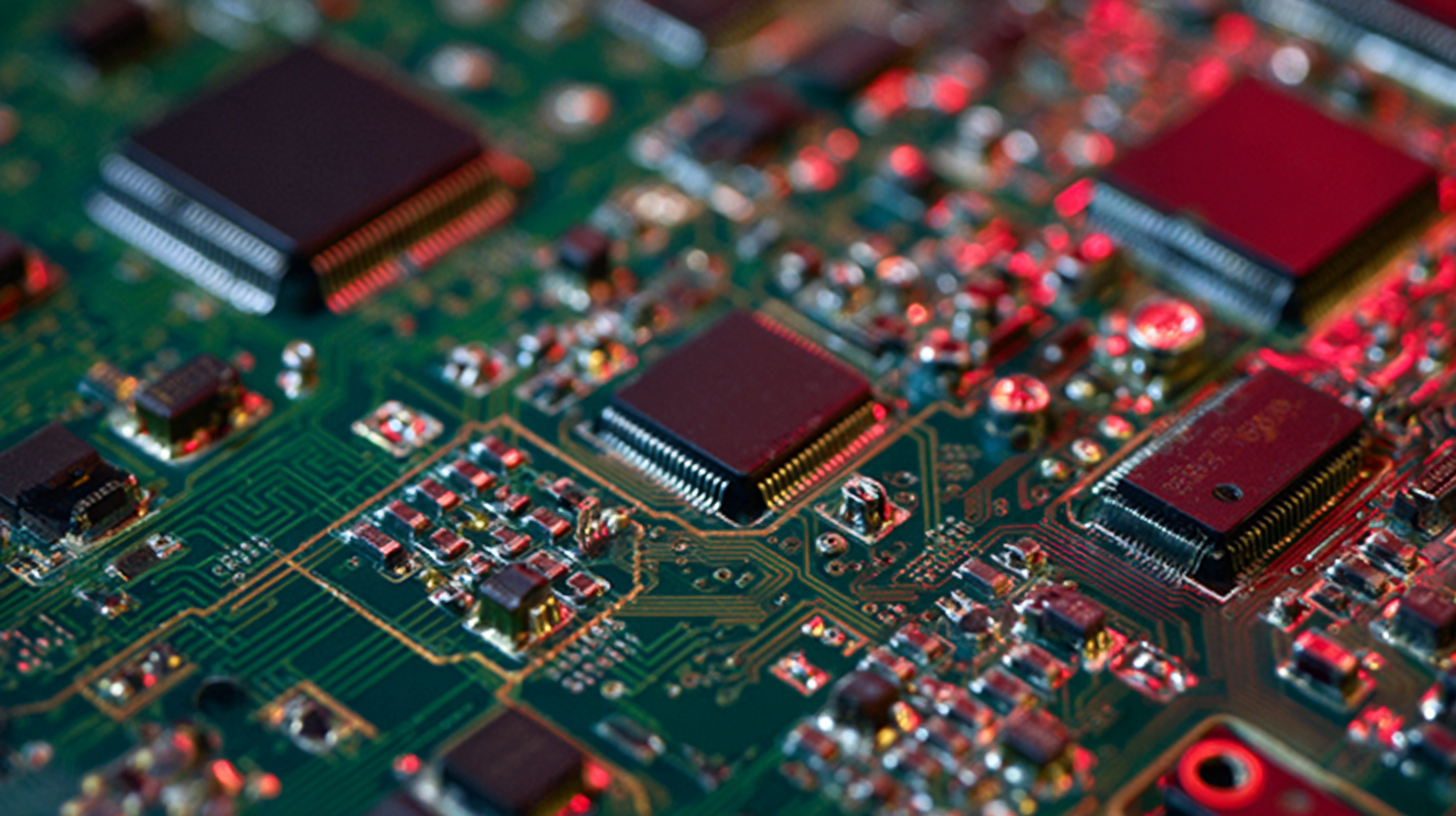
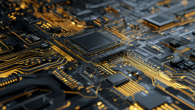
 Advanced PCBs, characterized by their high layer count, improved thermal management, and enhanced electrical performance,
are essential in meeting the rigorous requirements of contemporary electronic systems. As technology continues to evolve,
the role of advanced PCBs becomes increasingly critical, unlocking new possibilities and redefining the standards of innovation
in the electronics landscape.
Advanced PCBs, characterized by their high layer count, improved thermal management, and enhanced electrical performance,
are essential in meeting the rigorous requirements of contemporary electronic systems. As technology continues to evolve,
the role of advanced PCBs becomes increasingly critical, unlocking new possibilities and redefining the standards of innovation
in the electronics landscape.
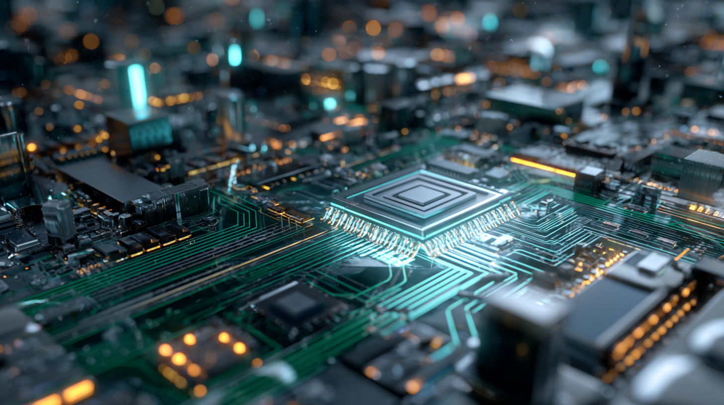
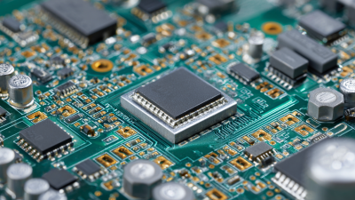
 The electronic landscape is transforming rapidly, with advanced PCBs at the core of this evolution. Miniaturization trends are driving efficiency and reliability across various industries. As devices continue to shrink, advanced PCBs are designed to meet the demanding specifications required for high-performance applications. These PCBs offer enhanced thermal management and high-density interconnects, making them ideal for modern electronic devices.
Moreover, the substrate-like PCB market is projected to experience significant growth, with a CAGR of 19.5%. By 2034, the market size is estimated to reach approximately USD 8.9 billion. This growth reflects the increasing demand for sophisticated electronic components that can accommodate complex designs and support emerging technologies.
Tips: When designing your PCB, consider using advanced design software that integrates AI for more efficient circuit layouts. Additionally, leverage tools that facilitate seamless collaboration between electronic design and mechanical design to optimize your workflow. Lastly, invest in defect detection methods to ensure high-quality production, as early identification of surface defects can greatly enhance overall product performance.
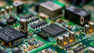
 In the realm of modern electronics, advanced printed circuit boards (PCBs) play a crucial role in innovation. The emergence of innovative manufacturing techniques has propelled next-generation PCBs, allowing for greater complexity and efficiency in electronic devices. Techniques such as additive manufacturing and automated assembly not only enhance precision but also reduce waste, making the production process more sustainable. These advancements enable the integration of high-density interconnects, which significantly reduce the size of electronic components while improving functionality.
Tips: When considering PCB design, prioritize the selection of materials that can withstand higher frequencies and temperatures. This is essential for ensuring that your designs remain reliable in the face of evolving technological demands. Additionally, stay informed about the latest advancements in PCB manufacturing processes, as they can provide competitive advantages in miniature and highly complex designs.
Moreover, the incorporation of smart manufacturing practices, like the Internet of Things (IoT), allows for real-time monitoring during the production. This can lead to quicker identification of issues and enhance overall quality. Embracing these innovative methods does not only streamline production but also facilitates the creation of more sophisticated electronic applications.
Tips: Collaborate closely with your manufacturing partners to discuss capabilities and limitations of new techniques, ensuring an aligned vision for your product development. Always prototype and test your designs to adapt swiftly to the continuously evolving electronic landscape.
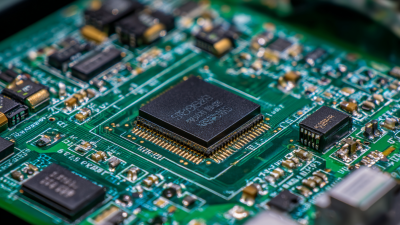
In the rapidly evolving landscape of modern electronics, advanced design strategies for printed circuit boards (PCBs) play a pivotal role in enhancing overall device performance. With the emergence of polymer semiconductors, particularly in the fields of organic lighting and photovoltaics, the integration of flexible materials into PCB design is revolutionizing how electronic devices are built. These advancements not only improve the mechanical properties of PCBs but also allow for innovative form factors that are crucial for portable devices.
Moreover, the advent of artificial intelligence in PCB engineering is transforming traditional design methodologies. As AI technologies mature, engineers are finding new ways to optimize the PCB layout process, enabling faster prototyping and more complex designs that meet the increasing demands of diverse electronic applications. This structural shift in the PCB industry is vital, as the global market continues to grow, driven by the need for high-density, low-cost, and reliable components. Adapting to these new strategies is essential for engineers looking to stay competitive in the ever-changing electronics sector.
| Dimension | Value | Impact on Electronics |
|---|---|---|
| Layer Count | 2 - 20+ | Increased functionality and compact design |
| Material Type | FR-4, Rogers, Polyimide | Improved performance in high-frequency applications |
| Surface Finish | ENIG, HASL, OSP | Enhanced solderability and shelf life |
| Impedance Control | 50 Ω, 75 Ω | Critical for high-speed signal integrity |
| Thermal Management | Thermal vias, metal core | Improved heat dissipation in dense designs |
| Packaging Type | BGA, QFN, CSP | Reduced footprint and enhanced performance |
Advanced printed circuit boards (PCBs) are pivotal in the evolution of modern electronics, enabling a wide array of applications that drive innovation in various fields. In the realm of telecommunications, advanced PCBs facilitate faster data transmission and improved signal integrity, essential for high-speed internet and 5G networks. Their intricate designs and multilayer configurations allow for compact and efficient transmission of signals, bolstering performance in smartphones and other communication devices.
Moreover, in the automotive industry, advanced PCBs are critical in the development of electric vehicles (EVs) and autonomous driving technologies. The incorporation of intelligent sensors, radar systems, and real-time data processing units within PCBs enhances safety and efficiency in modern vehicles. These boards not only reduce weight and size, enabling more streamlined designs, but they also support multifunctionality, accommodating various electronic components that contribute to the vehicle's overall performance.
In the medical sector, advanced PCBs are revolutionizing health monitoring and diagnostic equipment. Miniaturized PCBs are key in devices like wearable health trackers and portable diagnostic tools, allowing for continuous patient monitoring and real-time data analysis. Their reliability and precision directly impact patient outcomes, showcasing the transformative power of advanced PCB technology in health care and beyond.
The rapid evolution of technology is significantly driven by the advancements in printed circuit boards (PCBs). As the Internet of Things (IoT) and artificial intelligence (AI) continue to integrate deeply into our daily lives, the demand for sophisticated PCBs rises. These next-generation PCBs not only enhance connectivity and data transfer rates but also enable the miniaturization of devices. Their ability to support multiple functionalities within a compact design is crucial for IoT applications, where space and efficiency are paramount.
Moreover, advanced PCBs play a pivotal role in optimizing AI systems. With the increasing complexity of algorithms and the need for real-time processing, high-performance PCBs facilitate faster data processing and improved power management. The utilization of innovative materials and designs in these PCBs further supports advanced thermal management and signal integrity, ensuring reliable operation in AI frameworks. As both IoT and AI technologies advance, the evolution of PCBs will undoubtedly continue to be a key driver in realizing smarter, more connected environments.

„Thanks to the LUVIR technology, the solder resist process could be switched directly from the previously used mask exposure to direct exposure. As an outstanding digital solution on the market, this technology has been able to demonstrate fast process times and superior quality on our certified conventional ink in production. This allowed us to fully digitize the solder mask process at low cost – without process or ink adjustments. An excellent benefit to our production in Rot am See.“
Ralf Göhringer (Head of Production WE Rot am See)
I would definitely recommend the Limata machine and team for a future company purchase
Michael Greenaway
Compunetics Inc.
“The Limata ldi has been amazing!! Best thing we did was buy this machine”
Richard Brady
GM
Circuitlabs
“Since 2019, we have been running the Limata X1000 LDI system (including LUVIR for solder mask imaging) in daily production as an addition to our current process with film. The machine was capable of properly exposing Taiyo PSR-4000 BN (DI) solder mask types on normal to high-copper boards using a new and unique direct imaging process. The machine operating interface is very user friendly which allowed for a quick technical training curve. The pre-registration processing reduced several seconds of production time at every print. Limata support and service staff is incomparable. They supported our team every step of the way at basically any time of the day or night, with literally, an immediate response time, customizing the software interface to best fit our Operations and needs.
We have exposed more than 8,000 prints since end of October, on various solder mask colors and some resist film panels. Limata, has proven to be very capable and innovative. They are a strong contender in the industry.
We have very much enjoyed this project, and working with the team!
Thank you Limata for the continued support and being a part of our growth.”
Bill Sezate
Vice President, GM
Summit Interconnect
As a replacement to our current contact exposure process with film, the LIMATA X2000 system including LUVIR-Technology was capable of properly exposing non-LDI solder mask types using a direct imaging process. The machine offers cutting edge software with a very intuitive operating interface which allowed for quick technician training curve. The dual drawer system combined with pre-registration processing reduced several seconds of production time at every machine cycle. Limata support and service staff is world class. They added software patches to keep production running at shortest possible response times, customized the software interface to best fit our in-house Operations system, and even wrote a step-by-step machine processing manual. As a result of the project, we have exposed more than 16,000 times on various product types and solder mask brands/colors. Limata, in a very short timeframe as a company, has definitely shown they are truly innovative and will be challenging the industry of direct imaging for the top spot.
Kevin Beattie
Process Engineer
TTM Technologies
Forest Grove Division