Choosing the best PCB fabrication tools is crucial for successful electronic projects. The global PCB market is set to reach $75 billion by 2026, as reported by industry analysts. This rapid growth indicates a high demand for quality fabrication tools. These tools play a vital role in ensuring precision and reliability during the design and manufacturing stages of PCBs.
To make informed decisions, it's essential to evaluate various factors. Factors include tool compatibility, user-friendliness, and cost efficiency. Research shows that approximately 40% of engineering teams struggle with tool selection. This can lead to project delays and increased costs. Therefore, understanding the range of available options is critical.
Investing in the right PCB fabrication tools can enhance productivity. However, many still overlook crucial aspects during their selection process. They may prioritize brand over functionality, resulting in poor choices. This misjudgment can affect the overall quality of the final product. Proper guidance and a clear understanding of one’s specific needs are essential to avoid potential pitfalls.
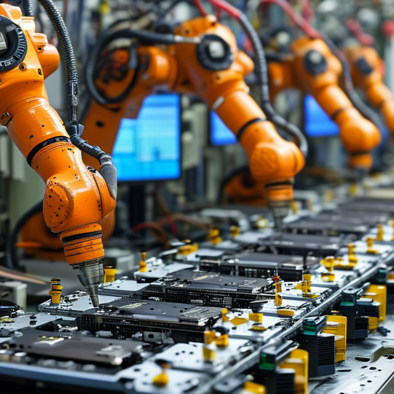
Understanding the PCB fabrication process is essential for engineers and designers. PCB fabrication involves several steps, including design, etching, drilling, and solder mask application. Each step influences the quality and functionality of the final product. Research from IPC shows that nearly 30% of PCBs fail due to production errors. This highlights the importance of precision in every phase.
The etching process is particularly critical. It determines the copper trace integrity. Using advanced software for design verification can mitigate common errors. However, many engineers still rely on traditional methods. This can lead to increased defects. A study by the International Electronics Manufacturing Initiative notes that 20% of projects face delays due to fabrication issues. Investing in modern tools can reduce such risks significantly.
Drilling is another area that requires attention. Poor drilling techniques can cause board delamination or pad damage. According to the Institute of Printed Circuits, over 15% of PCB defects arise during drilling. Awareness of these pitfalls is key. Continuous training and adopting new technologies can enhance fabrication quality and reduce costs. Hence, the right tools and processes are vital for achieving optimal results.
| Dimension | Details |
|---|---|
| Material Types | FR-4, CEM-1, Aluminum, Flexible materials |
| Layer Count | Single-sided, Double-sided, Multi-layer |
| Surface Finish | HASL, ENIG, Immersion Tin, OSP |
| Tolerance Levels | Standard (±0.1mm), Tight (±0.05mm) |
| Board Size | Custom sizes up to 600x1200 mm |
| Production Volume | Low-volume, High-volume, Prototyping |
| Lead Time | Standard (2-4 weeks), Expedited (1 week) |
| Testing Methods | Electrical Testing, Visual Inspection, Functional Testing |
When selecting PCB fabrication tools, certain essential features stand out. A robust design software is vital. It should support multi-layer designs and various PCB materials. According to industry reports, 70% of designers prioritize software that offers 3D visualization. This feature allows for better layout comprehension and error detection.
Another critical aspect is the accuracy of manufacturing tools. Precision is non-negotiable in PCB fabrication. Research shows that minute deviations can lead to significant failures. Tools offering a tolerance of ±0.1 mm are preferred by 68% of professionals. This level of accuracy ensures reliable performance in electronic applications.
User support and documentation can greatly impact the user experience. Effective resources enable users to navigate complex functions. A notable 65% of users report frustration with inadequate instruction manuals or technical support. Investing time in understanding these features is not just beneficial; it may help in avoiding costly errors down the road.
When selecting PCB fabrication tools, it's essential to understand the various types available. Each type serves a distinct purpose and offers unique features. For instance, manual tools are great for beginners. They provide hands-on experience but lack the precision of automated systems. On the other hand, advanced machines offer high precision and speed. However, they require significant investment and expertise.
In the realm of software tools, the choice is equally important. Schematic design software helps in visualizing circuits. In contrast, layout software optimizes component placement. This ensures better performance and manufacturability. Yet, both types can have steep learning curves. Many users may find them overwhelming initially. It's crucial to assess one's skill level before diving into complex software.
While comparing tools, consider budget and workflow. A high-end tool may promise superior results, but it can also lead to frustration if it doesn’t fit your process. Likewise, a cheaper tool might lack essential functions, limiting your capabilities. Balancing quality and functionality is key. This decision often involves trial and error, demanding reflection on past choices and future needs.
When evaluating PCB fabrication tools, cost-effectiveness is a crucial factor. It's essential to analyze both initial purchase costs and long-term expenses. Some tools may seem affordable at first glance, but hidden costs in maintenance can add up. Factor in material costs and potential wastage as well. A tool that saves money upfront might end up being costly over time, especially if it compromises quality.
Efficiency should also be at the forefront of your evaluation. Quick turnaround times and ease of use can boost productivity significantly. However, efficiency isn’t just about speed; it means maintaining precision in fabrication as well. A tool that speeds up production but delivers subpar results may lead to rework, ultimately skyrocketing costs.
It's beneficial to gather feedback from experienced users in the industry. Their insights can shed light on the reliability and performance of different tools. Remember, not every tool suits every project. Understanding your specific needs is vital for making informed decisions. Balancing cost and efficiency requires careful thought and strategic planning.
When selecting PCB fabrication tools, understanding your specific needs is crucial. The type of project influences tool choice significantly. For prototyping, a compact, user-friendly setup may suffice. Complexity and scale matter as well. Larger projects require tools with advanced features. Think about your skill level too. Beginner-friendly tools often offer guided processes, while seasoned professionals might prefer more customizable options.
Consider your budget and long-term goals. Investing in versatile tools can pay off. However, cheaper options may seem attractive but often lack reliability. Reflect on past experiences; quality differences can affect your workflow. It's essential to research various materials, from basic boards to advanced composites. Each material has unique requirements and implications for tool choice.
Evaluate user reviews and expert insights for guidance, although be wary of bias. Hands-on experience can be invaluable in understanding the nuances of the tools. Testing tools in real scenarios may reveal flaws you didn’t anticipate. This reflection can help refine your selection process. Always be open to reassessing your choices based on project feedback and outcomes.
„Thanks to the LUVIR technology, the solder resist process could be switched directly from the previously used mask exposure to direct exposure. As an outstanding digital solution on the market, this technology has been able to demonstrate fast process times and superior quality on our certified conventional ink in production. This allowed us to fully digitize the solder mask process at low cost – without process or ink adjustments. An excellent benefit to our production in Rot am See.“
Ralf Göhringer (Head of Production WE Rot am See)
I would definitely recommend the Limata machine and team for a future company purchase
Michael Greenaway
Compunetics Inc.
“The Limata ldi has been amazing!! Best thing we did was buy this machine”
Richard Brady
GM
Circuitlabs
“Since 2019, we have been running the Limata X1000 LDI system (including LUVIR for solder mask imaging) in daily production as an addition to our current process with film. The machine was capable of properly exposing Taiyo PSR-4000 BN (DI) solder mask types on normal to high-copper boards using a new and unique direct imaging process. The machine operating interface is very user friendly which allowed for a quick technical training curve. The pre-registration processing reduced several seconds of production time at every print. Limata support and service staff is incomparable. They supported our team every step of the way at basically any time of the day or night, with literally, an immediate response time, customizing the software interface to best fit our Operations and needs.
We have exposed more than 8,000 prints since end of October, on various solder mask colors and some resist film panels. Limata, has proven to be very capable and innovative. They are a strong contender in the industry.
We have very much enjoyed this project, and working with the team!
Thank you Limata for the continued support and being a part of our growth.”
Bill Sezate
Vice President, GM
Summit Interconnect
As a replacement to our current contact exposure process with film, the LIMATA X2000 system including LUVIR-Technology was capable of properly exposing non-LDI solder mask types using a direct imaging process. The machine offers cutting edge software with a very intuitive operating interface which allowed for quick technician training curve. The dual drawer system combined with pre-registration processing reduced several seconds of production time at every machine cycle. Limata support and service staff is world class. They added software patches to keep production running at shortest possible response times, customized the software interface to best fit our in-house Operations system, and even wrote a step-by-step machine processing manual. As a result of the project, we have exposed more than 16,000 times on various product types and solder mask brands/colors. Limata, in a very short timeframe as a company, has definitely shown they are truly innovative and will be challenging the industry of direct imaging for the top spot.
Kevin Beattie
Process Engineer
TTM Technologies
Forest Grove Division