In the rapidly evolving landscape of modern electronics, the significance of advanced PCBs (Printed Circuit Boards) cannot be overstated. According to a report by Market Research Future, the global PCB market is expected to reach $91 billion by 2025, with advanced PCBs driving substantial growth due to their ability to accommodate higher component densities and enhance thermal management. These sophisticated circuit boards are pivotal in diverse applications ranging from consumer electronics to automotive and aerospace industries. Their unique features, such as multi-layer structures, high-frequency capabilities, and improved material compositions, enable manufacturers to produce more compact and efficient devices.
This blog will delve into the distinct features and applications of the best advanced PCBs in modern electronics, showcasing their critical role in facilitating innovation and enhancing performance across various sectors.
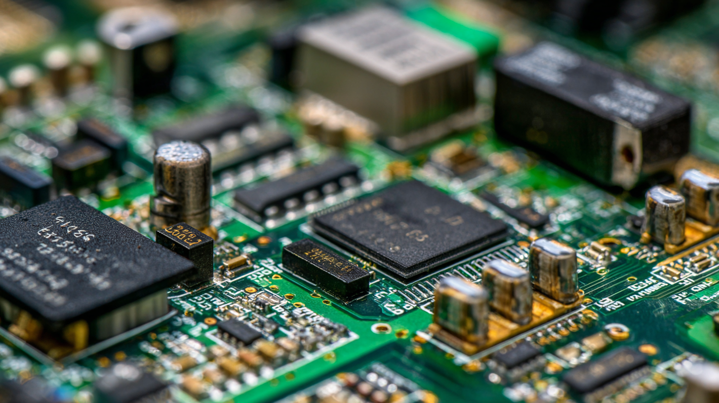
Advanced PCBs, or printed circuit boards, are integral to modern electronics, characterized by their high layer counts, complex geometries, and sophisticated materials. One of the key features that define these boards is their ability to handle higher frequencies and improved signal integrity. This characteristic is crucial for applications in telecommunications, where minimizing signal loss and electromagnetic interference is paramount. Advanced PCBs often utilize materials such as high-frequency laminates and copper with enhanced conductivity to facilitate superior performance.
Another defining characteristic of advanced PCBs is their thermal management capabilities. As electronic devices become more compact and powerful, the need for effective heat dissipation becomes critical. Advanced PCBs are designed with thermal vias and built-in heat sinks that enable efficient heat transfer, ensuring components operate within safe temperature ranges. Additionally, features like microvias and blind/buried vias allow for denser circuit layouts without sacrificing performance, making them suitable for high-density interconnect (HDI) applications. These advancements not only enhance the functionality of electronics but also pave the way for innovations in fields such as automotive technology and consumer gadgets.
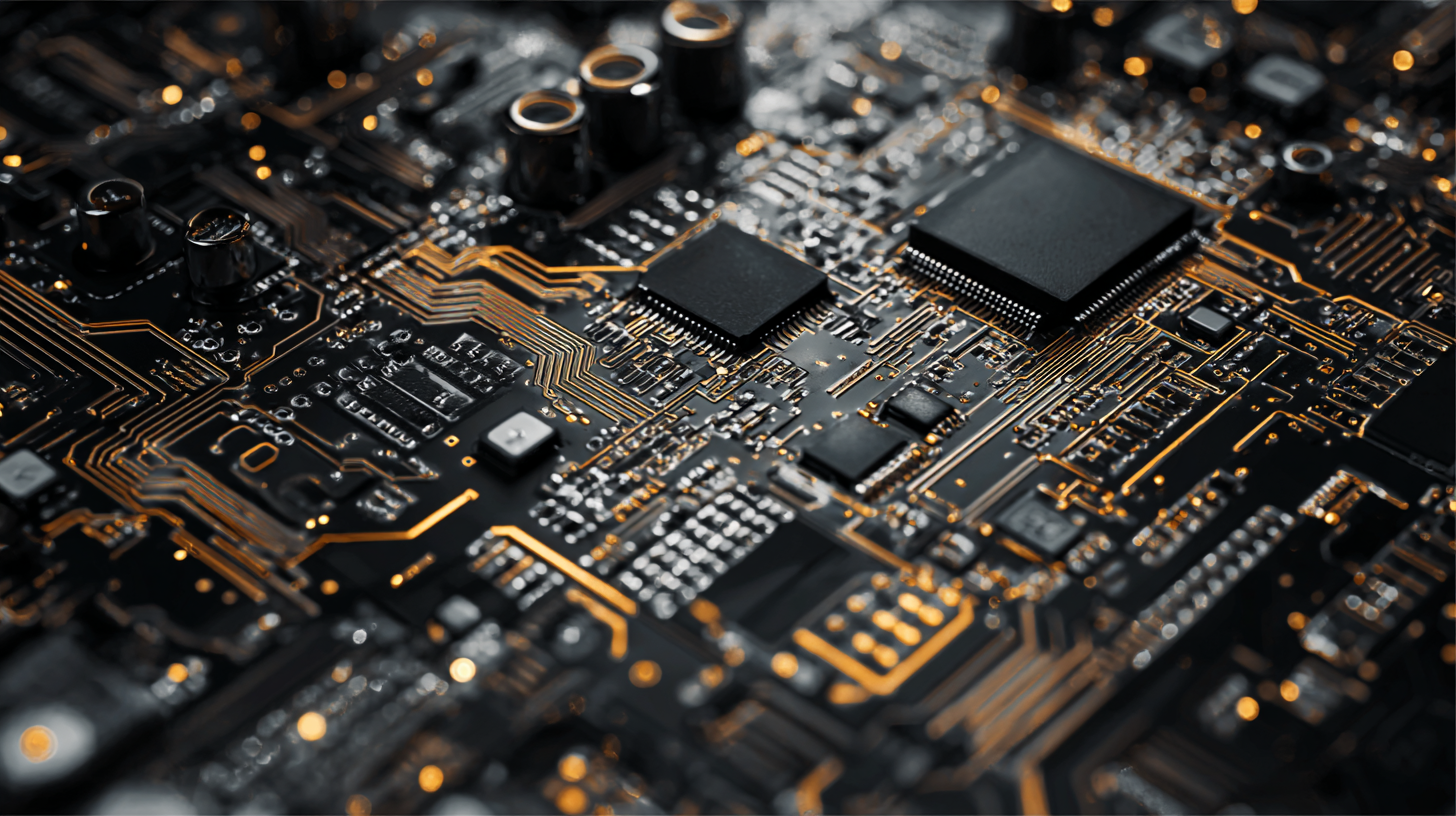
When it comes to advanced printed circuit boards (PCBs), understanding the various types and their applications is essential for modern electronics. From rigid PCBs to flexible and rigid-flex designs, each type offers distinct advantages. Rigid PCBs, commonly used in devices such as smartphones and computers, provide robust support for components but lack flexibility. Conversely, flexible PCBs enable intricate designs and can conform to various shapes, making them perfect for wearable technology.
Tip: When selecting a PCB type, consider the size constraints and environmental factors of your project. For instance, if your gadget needs to be compact and lightweight, flexible PCBs could be the best choice.
Additionally, there are high-frequency and high-density interconnect (HDI) PCBs, designed for complex electronic applications like telecommunications and advanced computing. These PCBs support high-speed signals and require precise manufacturing techniques. Implementing these technologies can significantly enhance the performance and reliability of electronic systems.
Tip: Evaluating the thermal management and signal integrity requirements during the design phase can lead to better performance in HDI applications, ensuring that the advanced PCBs meet the rigorous demands of modern electronics.
The advent of advanced Printed Circuit Boards (PCBs) has transformed the landscape of modern electronics, enabling innovative applications across various emerging technologies. From the rapidly evolving fields of AI and IoT to renewable energy solutions, advanced PCBs facilitate higher efficiency, miniaturization, and enhanced functionality. For instance, in electric vehicles, specialized PCBs are designed to handle high voltages and integrate seamlessly with battery management systems, promoting safer and more efficient energy usage.
When integrating advanced PCBs into new projects, it’s essential to consider design intricacies early in the development process. **Tip:** Use simulation software to visualize the PCB layout and anticipate potential issues before manufacturing. This tool can save time and reduce costs by identifying problems that might arise with component placement or heat dissipation.
In the medical field, advanced PCBs play a crucial role in the development of wearable health monitoring devices. These PCBs not only provide the necessary circuitry but also allow for the integration of advanced sensors that track vital signs in real-time. **Tip:** Prioritize flexibility in your PCB design to accommodate the unique requirements of compact medical devices without compromising durability. This approach ensures that devices remain reliable even in challenging environments.
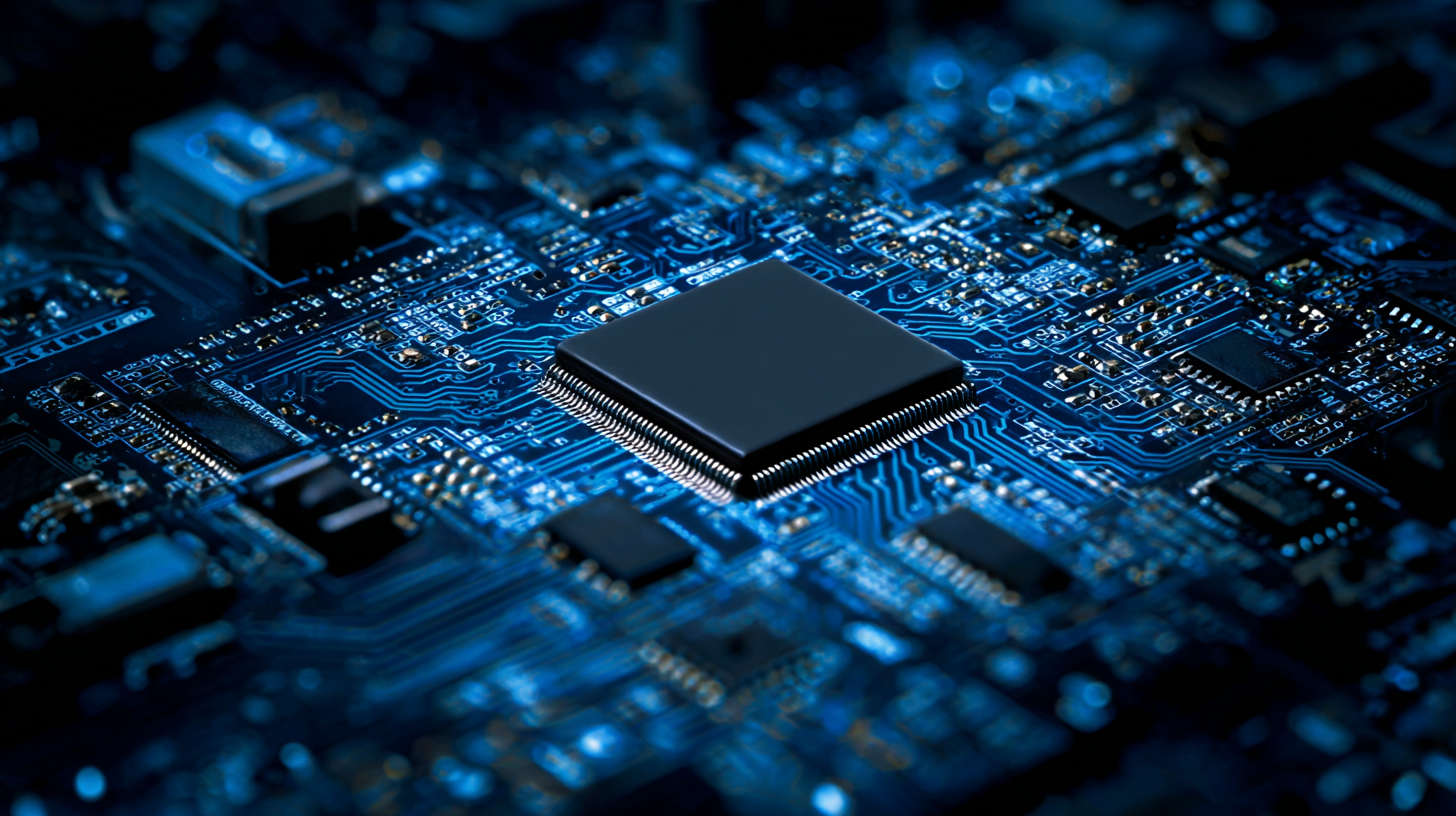
When it comes to designing and manufacturing high-quality printed circuit boards (PCBs), a well-structured approach is essential. One crucial tip is to ensure that your design software is based on industry standards. Utilizing advanced EDA tools can help streamline the design process, prevent layout errors, and enhance traceability. Make sure to review your design rules meticulously to avoid potential pitfalls later in the production phase.
Another important aspect is the choice of materials. Selecting the right substrate can significantly impact the performance and durability of the PCB. For high-frequency applications, consider using materials with low dielectric constant and loss. Additionally, ensuring that you’re sourcing components from reputable suppliers can mitigate risks associated with counterfeit parts and lead to better overall circuit reliability.
Lastly, incorporating thorough testing procedures throughout the manufacturing process is vital. This could involve utilizing automated optical inspection (AOI) and electrical testing (ICT) to identify defects early on. By prioritizing quality assurance from the design phase to final assembly, you can enhance the performance of your PCBs and ensure they meet the rigorous demands of modern electronics.
The global automotive PCB market is anticipated to see significant growth, expanding from $9.15 billion in 2023 to $15.1 billion by 2032, with a compound annual growth rate (CAGR) of 5.9%. This trend is indicative of the overall advancements in electronics, driven by the increasing demand for advanced PCB technologies. As industries evolve, the need for higher density and more efficient circuit boards becomes essential. The shift towards lightweight and compact electronic products is propelling the development of technologies such as High-Density Interconnect (HDI) PCBs, which facilitate smaller apertures and finer line widths.
As we look toward the future, several key trends will shape the advancement of PCB technology. One notable area is embedded power modules, which integrate power chips directly into the PCBs to enhance performance and reliability. Additionally, collaborative robotics are expected to revolutionize manufacturing processes, pushing for more sophisticated and flexible PCB applications. Designers and engineers need to stay ahead of these trends to ensure their products meet the demands of modern electronics.
**Tips:**
1. Stay updated on emerging technologies, such as HDI and embedded modules, to leverage their capabilities in your designs.
2. Consider future applications and scalability when selecting PCB technologies to ensure longevity and adaptability in your projects.
„Thanks to the LUVIR technology, the solder resist process could be switched directly from the previously used mask exposure to direct exposure. As an outstanding digital solution on the market, this technology has been able to demonstrate fast process times and superior quality on our certified conventional ink in production. This allowed us to fully digitize the solder mask process at low cost – without process or ink adjustments. An excellent benefit to our production in Rot am See.“
Ralf Göhringer (Head of Production WE Rot am See)
I would definitely recommend the Limata machine and team for a future company purchase
Michael Greenaway
Compunetics Inc.
“The Limata ldi has been amazing!! Best thing we did was buy this machine”
Richard Brady
GM
Circuitlabs
“Since 2019, we have been running the Limata X1000 LDI system (including LUVIR for solder mask imaging) in daily production as an addition to our current process with film. The machine was capable of properly exposing Taiyo PSR-4000 BN (DI) solder mask types on normal to high-copper boards using a new and unique direct imaging process. The machine operating interface is very user friendly which allowed for a quick technical training curve. The pre-registration processing reduced several seconds of production time at every print. Limata support and service staff is incomparable. They supported our team every step of the way at basically any time of the day or night, with literally, an immediate response time, customizing the software interface to best fit our Operations and needs.
We have exposed more than 8,000 prints since end of October, on various solder mask colors and some resist film panels. Limata, has proven to be very capable and innovative. They are a strong contender in the industry.
We have very much enjoyed this project, and working with the team!
Thank you Limata for the continued support and being a part of our growth.”
Bill Sezate
Vice President, GM
Summit Interconnect
As a replacement to our current contact exposure process with film, the LIMATA X2000 system including LUVIR-Technology was capable of properly exposing non-LDI solder mask types using a direct imaging process. The machine offers cutting edge software with a very intuitive operating interface which allowed for quick technician training curve. The dual drawer system combined with pre-registration processing reduced several seconds of production time at every machine cycle. Limata support and service staff is world class. They added software patches to keep production running at shortest possible response times, customized the software interface to best fit our in-house Operations system, and even wrote a step-by-step machine processing manual. As a result of the project, we have exposed more than 16,000 times on various product types and solder mask brands/colors. Limata, in a very short timeframe as a company, has definitely shown they are truly innovative and will be challenging the industry of direct imaging for the top spot.
Kevin Beattie
Process Engineer
TTM Technologies
Forest Grove Division