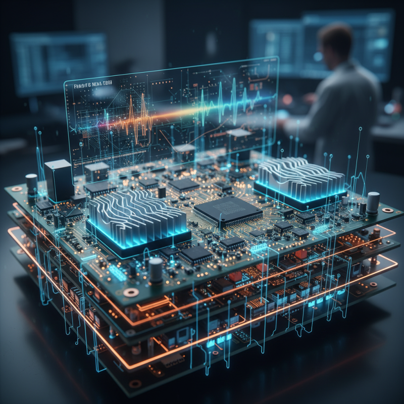
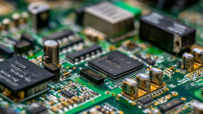
In the rapidly evolving world of electronics, mastering advanced PCB design techniques is crucial for performance enhancement. Dr. Emily Chang, a leading expert in advanced PCB technology, once stated, "The path to innovation lies in our ability to push the boundaries of PCB design." This sentiment resonates deeply with engineers striving to create efficient and reliable circuit boards.
Advanced PCB design goes beyond traditional methods. It requires a solid understanding of materials, thermal management, and signal integrity. Designers face challenges while navigating the complexities of multilayer boards and high-frequency signals. Each decision can significantly affect performance. Even experienced engineers can encounter unexpected issues that demand innovative solutions.
To achieve excellence, one must embrace continuous learning. Understanding the latest tools and techniques is essential. Engineers should also be open to feedback and willing to adjust their approaches. Advanced PCB design is not without its hurdles, but it presents opportunities for growth and innovation. By focusing on these areas, designers can elevate their work and contribute to cutting-edge technology.
Understanding the fundamentals of PCB design is crucial for anyone in electronics. A printed circuit board is more than just a physical support for components. It acts as a vital link between different elements of a device.
Effective PCB design starts with proper layout planning. The placement of components impacts signal integrity. Consider how traces connect and the lengths involved. The distance matters too. Shorter traces can reduce noise and interference. Yet, achieving an ideal layout is often challenging. Designers must regularly assess trade-offs. Component density versus heat dissipation, for example, can lead to tough decisions.
The importance of thorough testing cannot be overstated. A well-designed PCB needs validation. However, not every design passes the first test. Designers should remain open to feedback and willing to iterate. It is essential to review designs critically. Improvement is a journey; learning from mistakes enhances skills. Embracing imperfections can lead to better performance in future projects.
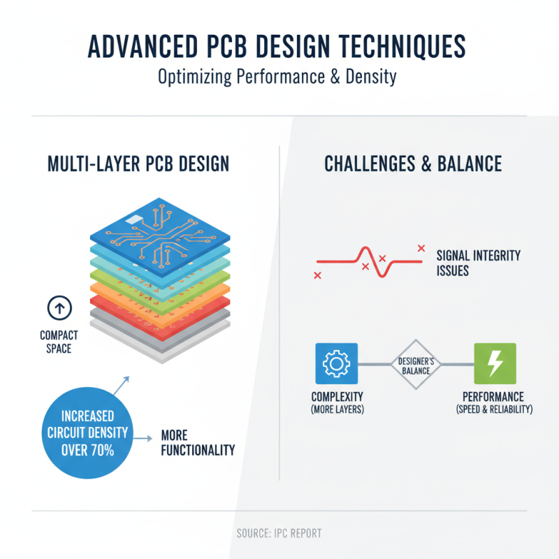
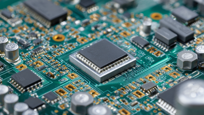
In today's fast-paced electronics environment, advanced PCB design techniques are crucial for performance enhancements. One key technique is multi-layer PCB design, which allows for increased functionality in a compact space. A report from IPC shows that multi-layer boards increase circuit density by over 70%. However, more layers can lead to issues with signal integrity. Designers must strike a balance between complexity and performance.
Another technique gaining traction is the use of embedded components. This approach can save space and reduce manufacturing costs. According to a study by TechSearch International, PCBs with embedded components can minimize assembly costs by roughly 25%. It's essential, however, to ensure thermal management is adequate, as embedded components may lead to heat accumulation.
**Tip:** Always analyze thermal profiles early in the design phase. Address potential hotspots to avoid performance degradation later.
Lastly, differential signaling is vital for high-speed designs. It mitigates noise and enhances signal quality. Reports from IEEE indicate that differential pairs can improve electromagnetic compatibility by up to 15%. Yet, improper implementation can introduce crosstalk. Careful routing is necessary to maximize benefits while preventing interference.
**Tip:** Keep differential pairs as short and close together as possible to reduce crosstalk. This subtlety makes a significant difference.
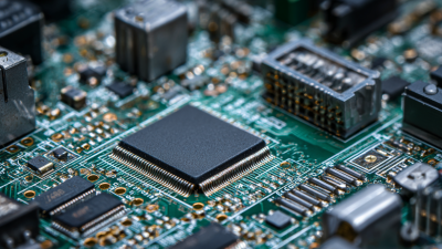
Integrating high-frequency components in PCB design can significantly enhance signal integrity. High-frequency signals are susceptible to interference and loss. Therefore, careful attention to layout and component placement is crucial. Components should be placed close to each other to minimize the length of signal paths. The trace width and spacing also matter greatly.
When dealing with high frequencies, pay attention to the ground plane. A solid ground plane reduces return path issues. Ensure that all high-frequency components have a direct path to the ground. This is often overlooked and can lead to performance degradation.
**Tip:** Use differential pairs for critical signals. This can drastically improve noise immunity.
Additionally, consider the dielectric material of your PCB. Materials with low loss characteristics help maintain signal integrity at high frequencies. Fiber glass, for instance, may not perform well in high-frequency applications.
**Tip:** Simulate your design before fabrication. This allows you to identify potential issues early. Mistakes can be costly, and corrections must be made in design stages.
It is essential to keep in mind that not all designs come out perfect. Feedback from prototypes can reveal unforeseen problems. Constant reflection on your design choices can lead to improved performance in subsequent iterations.
An efficient PCB design workflow is crucial for mastering advanced PCB design techniques. Organizing your work can reduce errors and boost performance. Start by selecting the right software tools. These tools can help streamline tasks like schematic capture, layout, and simulation. With a solid environment in place, designers can focus more on innovation.
Utilizing software effectively means understanding its limitations. Some tools may not support advanced features you need. It’s frustrating when software crashes or doesn't perform as expected. Regularly update your tools to mitigate such issues. You might also face a learning curve; take time to explore all functionalities. This can significantly enhance your design capabilities.
Moreover, collaboration within teams can boost efficiency. Using cloud-based tools allows multiple users to access designs simultaneously. Yet, communication can be a challenge. Seek feedback from peers early in the design phase. This can help identify flaws before they become larger problems. A well-designed PCB is not just about the layout—it's about the overall workflow and teamwork.
| Technique | Description | Software Tools | Benefits |
|---|---|---|---|
| Signal Integrity Analysis | Ensures that the electrical signals transmitted through PCB traces are clear and unaffected by noise. | Altium Designer, HyperLynx | Improved performance and reliability of the circuit. |
| Thermal Analysis | Assesses heat distribution and dissipation within the PCB design to prevent overheating. | ANSYS, SolidWorks Simulation | Enhances longevity and performance consistency. |
| Layer Stackup Optimization | Strongly influences impedance control and overall board performance. | Cadence, KiCad | Improves signal integrity and reduces manufacturing costs. |
| Design Rule Checking (DRC) | Automatically checks for design errors based on predefined manufacturing rules. | EAGLE, Altium Designer | Minimizes errors and reduces production delays. |
| Routing Optimization | Enhances the trace layout for reduced capacitance and inductance. | OrCAD, Altium Designer | Increases efficiency and signal quality. |
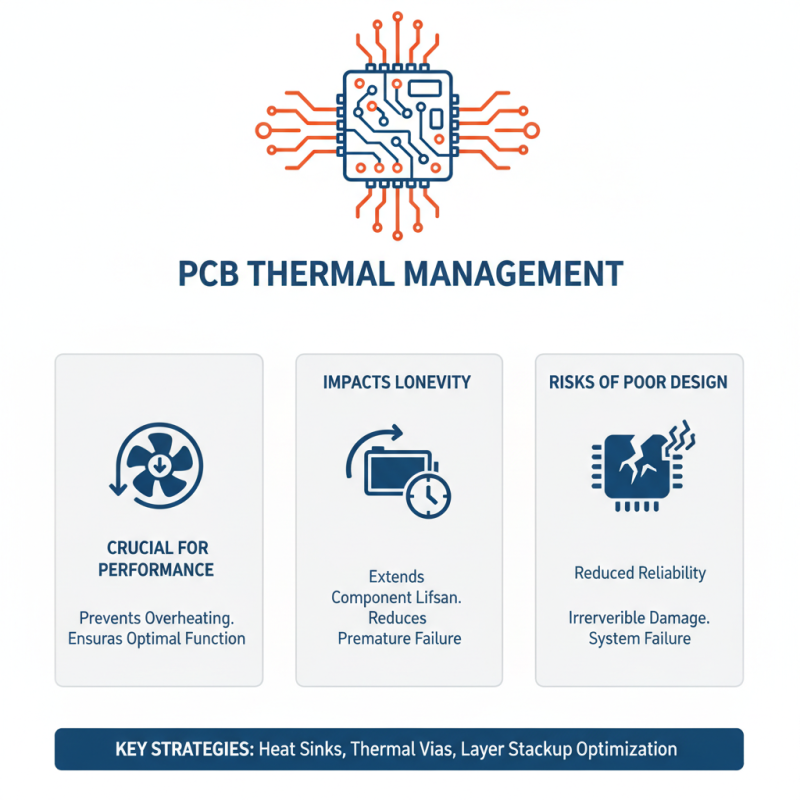
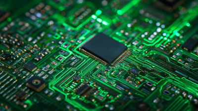
Effective thermal management is crucial in PCB design. Heat dissipation affects the performance and longevity of electronic components. Poor thermal strategies lead to overheating, which can cause failure.
To implement effective thermal management, consider the layout's complexity. Place heat-sensitive components away from heat-generating parts. Use thermal vias and large pads to transfer heat away efficiently. Pay attention to the material used for thermal conductivity. Materials like copper have better heat transfer properties compared to others.
Reflecting on design choices can reveal potential pitfalls. For example, dense component placement might hinder airflow. This can trap heat, worsening performance. Regularly reviewing thermal simulations can help identify and mitigate such issues. In some cases, revisiting the layout and component choice becomes necessary to enhance overall thermal performance.

„Thanks to the LUVIR technology, the solder resist process could be switched directly from the previously used mask exposure to direct exposure. As an outstanding digital solution on the market, this technology has been able to demonstrate fast process times and superior quality on our certified conventional ink in production. This allowed us to fully digitize the solder mask process at low cost – without process or ink adjustments. An excellent benefit to our production in Rot am See.“
Ralf Göhringer (Head of Production WE Rot am See)
I would definitely recommend the Limata machine and team for a future company purchase
Michael Greenaway
Compunetics Inc.
“The Limata ldi has been amazing!! Best thing we did was buy this machine”
Richard Brady
GM
Circuitlabs
“Since 2019, we have been running the Limata X1000 LDI system (including LUVIR for solder mask imaging) in daily production as an addition to our current process with film. The machine was capable of properly exposing Taiyo PSR-4000 BN (DI) solder mask types on normal to high-copper boards using a new and unique direct imaging process. The machine operating interface is very user friendly which allowed for a quick technical training curve. The pre-registration processing reduced several seconds of production time at every print. Limata support and service staff is incomparable. They supported our team every step of the way at basically any time of the day or night, with literally, an immediate response time, customizing the software interface to best fit our Operations and needs.
We have exposed more than 8,000 prints since end of October, on various solder mask colors and some resist film panels. Limata, has proven to be very capable and innovative. They are a strong contender in the industry.
We have very much enjoyed this project, and working with the team!
Thank you Limata for the continued support and being a part of our growth.”
Bill Sezate
Vice President, GM
Summit Interconnect
As a replacement to our current contact exposure process with film, the LIMATA X2000 system including LUVIR-Technology was capable of properly exposing non-LDI solder mask types using a direct imaging process. The machine offers cutting edge software with a very intuitive operating interface which allowed for quick technician training curve. The dual drawer system combined with pre-registration processing reduced several seconds of production time at every machine cycle. Limata support and service staff is world class. They added software patches to keep production running at shortest possible response times, customized the software interface to best fit our in-house Operations system, and even wrote a step-by-step machine processing manual. As a result of the project, we have exposed more than 16,000 times on various product types and solder mask brands/colors. Limata, in a very short timeframe as a company, has definitely shown they are truly innovative and will be challenging the industry of direct imaging for the top spot.
Kevin Beattie
Process Engineer
TTM Technologies
Forest Grove Division