In the rapidly evolving landscape of electronics manufacturing, optimizing the PCB process has become paramount for companies seeking to enhance productivity and reduce costs. According to a report from the IPC Association Connecting Electronics Industries, improving PCB manufacturing efficiency can lead to reductions in production time by as much as 30%. As the demand for more complex and miniaturized electronic devices continues to rise, the pressure on manufacturers to adopt advanced techniques has never been greater.

Renowned PCB process expert, Dr. Emily Chen, emphasizes this point by stating, "The key to staying competitive in today's market lies in the continuous optimization of PCB processes through innovative technologies." Her insights echo the need for manufacturers to invest in advanced methodologies, including automation, machine learning, and real-time data analytics, which are all critical components that can significantly enhance PCB production efficiency. By embracing these advanced practices, companies can not only streamline their operations but also position themselves at the forefront of the industry, ready to meet the challenges of tomorrow's electronic demands.
Implementing lean manufacturing strategies in PCB production can significantly increase output and efficiency. By focusing on waste reduction and continuous improvement, manufacturers can streamline their processes and ensure that resources are utilized effectively. One key strategy is to adopt a just-in-time (JIT) approach, which minimizes inventory costs and allows for more agility in meeting customer demands. This method ensures a steady flow in production without the burden of excess materials.
Tips: Start by mapping your current processes to identify bottlenecks and areas of waste. Use Lean tools such as Value Stream Mapping to visualize the flow of materials and information in your PCB production line. This will help you pinpoint inefficiencies that can be addressed.
Another effective lean strategy is to implement standardized work procedures. By establishing clear guidelines for operations, workers can perform tasks with consistent quality and efficiency. This not only simplifies training for new employees but also facilitates ongoing improvement as the team can readily identify deviations from established standards.
Tips: Conduct regular training sessions to reinforce standard operating procedures and encourage feedback from employees on potential improvements. Creating a culture of continuous improvement engages the entire team in the optimization process, leading to increased productivity and a more responsive production environment.
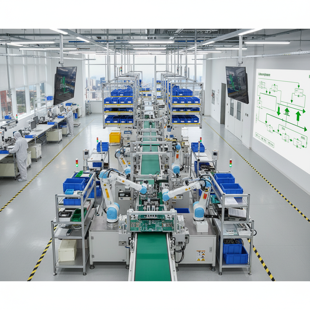
The adoption of automation and AI technologies is revolutionizing PCB assembly processes, significantly enhancing efficiency and productivity. Recent insights from Productronica emphasize a shift towards smart factory technologies and data-driven manufacturing. With automation leading the charge, it is projected that manufacturers can boost their operational efficiency by up to 30% by implementing these advanced techniques. A report from leading industry analysts indicates that companies leveraging AI for predictive maintenance and quality control are witnessing a return on investment that justifies these transitions—highlighting the potential of smart applications in manufacturing to reduce downtime and streamline workflows.
In the automotive sector, the integration of AI in manufacturing processes is particularly transformative. Companies are harnessing predictive analytics and autonomous robotics to drive precision and adaptability in production lines, ensuring not just efficiency but also higher quality outputs. The automation in electronic manufacturing services is on the rise, with market research showing that the sector is projected to grow significantly by 2034 as firms increasingly adopt robotics and AI technologies. These advancements promise a new era where operational bottlenecks are minimized, allowing organizations to respond rapidly to market demands while maintaining competitive advantage.
This chart illustrates the expected efficiency improvements in the PCB assembly process when adopting advanced automation and AI technologies. The current efficiency level is set at 70%, with significant gains projected through the integration of automation and AI, culminating in an overall efficiency of 100%.
In the competitive landscape of PCB fabrication, real-time data analytics emerges as a transformative tool for optimizing supply chain management. By leveraging data-driven insights, manufacturers can track inventory levels, predict material needs, and respond to demand fluctuations with agility. This approach not only minimizes delays but also reduces waste, ensuring that the right materials are available at the right time.
Tip 1: Implement dashboards that visualize key performance metrics, allowing teams to monitor real-time data and make informed decisions quickly.
Utilizing advanced analytics also enables manufacturers to identify bottlenecks and streamline processes. By analyzing workflows and supply chain performance, companies can gain a deeper understanding of their operations, leading to smarter procurement choices and a more efficient production cycle.
Tip 2: Regularly review analytics reports to pinpoint areas for improvement within the supply chain, creating a feedback loop that encourages continuous optimization.
Furthermore, integrating predictive analytics can facilitate proactive supply chain management. By anticipating future challenges based on historical data, manufacturers can take preventive actions, reducing the risk of disruptions and enhancing overall efficiency.
Tip 3: Foster collaboration across departments to ensure that insights gained from data analytics are shared and acted upon, enhancing the responsiveness of the entire organization.

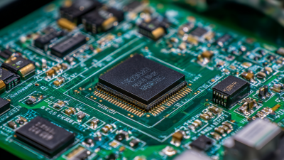
The aerospace materials market is set to reach an estimated value of $40.27 billion in 2023, with a compound annual growth rate (CAGR) of 8.82% forecasted from 2024 to 2031. This robust growth underscores the increasing emphasis on advanced materials, which play a crucial role in optimizing PCB processes. The evolution of PCB technology heavily relies on incorporating these materials to enhance performance and production efficiency.
Advanced materials not only improve the physical properties of PCBs but also contribute to more streamlined manufacturing processes. For instance, the introduction of innovative photoresists is projected to boost the PCB photoresist market to $7.2 billion by 2032, with a CAGR of 3.34% from 2024 to 2032. This shift to high-performance materials allows manufacturers to produce more reliable and efficient PCBs, ultimately leading to a 30% increase in overall production efficiency.
Tips: Consider investing in training programs for your workforce to familiarize them with new materials and techniques. Emphasizing modern design and manufacturing practices will facilitate smoother transitions when integrating advanced materials into your PCB production processes. Additionally, keep an eye on industry trends to adapt your strategies and maintain competitive advantage.
Design for Manufacturability (DFM) principles play a crucial role in PCB production, as they focus on enhancing the manufacturability of electronic components while minimizing waste and reducing production costs. According to a recent study by the IPC, the adoption of DFM strategies can lead to up to a 30% increase in production efficiency. By addressing potential manufacturing challenges during the design phase, engineers can mitigate issues that may arise during assembly, thus avoiding costly rework and waste.
One effective DFM technique involves simplifying the PCB layout. By optimizing component placement and minimizing trace lengths, designers can reduce the risk of signal integrity issues and improve throughput. Additionally, utilizing standard components whenever possible helps streamline procurement and manufacturing processes. This strategic planning not only minimizes waste but also can result in significant time savings, ultimately enhancing overall productivity.
Tips: Consider incorporating design software that emphasizes DFM capabilities early in the design phase. Regular training sessions for your engineering team on the latest DFM guidelines can also foster a culture of efficiency and innovation. Lastly, collaborating closely with manufacturers from the outset ensures that your designs are aligned with production capabilities, further reducing the likelihood of errors and waste.


„Thanks to the LUVIR technology, the solder resist process could be switched directly from the previously used mask exposure to direct exposure. As an outstanding digital solution on the market, this technology has been able to demonstrate fast process times and superior quality on our certified conventional ink in production. This allowed us to fully digitize the solder mask process at low cost – without process or ink adjustments. An excellent benefit to our production in Rot am See.“
Ralf Göhringer (Head of Production WE Rot am See)
I would definitely recommend the Limata machine and team for a future company purchase
Michael Greenaway
Compunetics Inc.
“The Limata ldi has been amazing!! Best thing we did was buy this machine”
Richard Brady
GM
Circuitlabs
“Since 2019, we have been running the Limata X1000 LDI system (including LUVIR for solder mask imaging) in daily production as an addition to our current process with film. The machine was capable of properly exposing Taiyo PSR-4000 BN (DI) solder mask types on normal to high-copper boards using a new and unique direct imaging process. The machine operating interface is very user friendly which allowed for a quick technical training curve. The pre-registration processing reduced several seconds of production time at every print. Limata support and service staff is incomparable. They supported our team every step of the way at basically any time of the day or night, with literally, an immediate response time, customizing the software interface to best fit our Operations and needs.
We have exposed more than 8,000 prints since end of October, on various solder mask colors and some resist film panels. Limata, has proven to be very capable and innovative. They are a strong contender in the industry.
We have very much enjoyed this project, and working with the team!
Thank you Limata for the continued support and being a part of our growth.”
Bill Sezate
Vice President, GM
Summit Interconnect
As a replacement to our current contact exposure process with film, the LIMATA X2000 system including LUVIR-Technology was capable of properly exposing non-LDI solder mask types using a direct imaging process. The machine offers cutting edge software with a very intuitive operating interface which allowed for quick technician training curve. The dual drawer system combined with pre-registration processing reduced several seconds of production time at every machine cycle. Limata support and service staff is world class. They added software patches to keep production running at shortest possible response times, customized the software interface to best fit our in-house Operations system, and even wrote a step-by-step machine processing manual. As a result of the project, we have exposed more than 16,000 times on various product types and solder mask brands/colors. Limata, in a very short timeframe as a company, has definitely shown they are truly innovative and will be challenging the industry of direct imaging for the top spot.
Kevin Beattie
Process Engineer
TTM Technologies
Forest Grove Division