In the world of printed circuit boards (PCBs), the role of a solder mask PCB is crucial for ensuring optimal performance and longevity of electronic devices. The solder mask, a protective layer applied to the surface of PCBs, serves multiple purposes beyond mere aesthetics. It not only helps to prevent solder bridges during assembly but also protects the circuit board from environmental factors such as moisture, dust, and corrosion. This makes understanding the intricacies of solder mask PCB essential for both manufacturers and engineers alike.
As technology continues to advance, the demands placed on PCBs have evolved, leading to the development of various solder mask options tailored for specific applications. Selecting the right solder mask PCB can significantly enhance the reliability and functionality of electronic products. Factors such as thermal stability, chemical resistance, and dielectric properties are pivotal considerations that must be taken into account in the design and manufacturing process. By delving deeper into the characteristics and benefits of solder mask PCBs, stakeholders can make informed decisions that ultimately contribute to superior electronic performance.
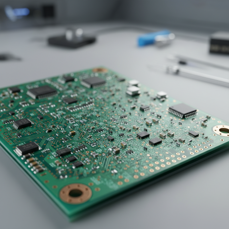
Solder mask is a crucial component in printed circuit board (PCB) manufacturing, serving as a protective layer that insulates copper traces and prevents solder bridges during assembly. The primary purpose of solder mask is to ensure optimal performance by shielding the conductive pathways from environmental factors and mechanical wear. Its application not only enhances the longevity of PCBs but also improves reliability, particularly in intricate designs like ball-grid arrays (BGAs), where ultra-fine pitch devices pose significant design challenges.
Recent advancements in solder mask technology have introduced innovations such as inkjet applications, which offer potential for high-volume production and customization. Different solder mask colors can also contribute to the aesthetic and functional aspects of PCB design, with options ranging from classic green to vibrant hues like red and blue. Additionally, studies on solder paste transfer efficiency underscore the critical role this masking layer plays in overall fabrication success, emphasizing the importance of factors like powder size and stencil quality in achieving precise solder applications. As the industry progresses, understanding the nuances of solder mask will be vital for engineers seeking to push the boundaries of PCB performance.
Solder masks play a crucial role in enhancing the performance of printed circuit boards (PCBs) by preventing solder bridging and ensuring reliable electrical connections. There are several types of solder masks, primarily categorized by the materials used. The most common types include epoxy, liquid photoimageable, and flexible solder masks. Each material has unique properties, making them suitable for specific applications. For instance, epoxy solder masks provide excellent chemical resistance, making them ideal for harsh environments, while liquid photoimageable masks offer high resolution for fine pitch designs.
The solder materials market is projected to witness significant growth, with the demand for lead-free solder expected to increase substantially. According to recent market analysis, the global solder materials market is anticipated to reach a market size of USD 55.0 million in the UK alone by 2035, reflecting a CAGR of 3.9% during the forecast period. This growth is driven by increasing regulations favoring lead-free solder options and advancements in solder technology, such as the development of anisotropic microcomposite joints that enhance connectivity in high-temperature applications. As manufacturers continue to innovate, the choice of solder mask material will be essential to optimize performance and ensure longevity in electronic devices.
| Solder Mask Type | Material | Applications | Key Features |
|---|---|---|---|
| Epoxy Solder Mask | Epoxy resin | Consumer electronics, automotive | Good adhesion, chemical resistance |
| Liquid Photoimageable (LPI) Solder Mask | Photoimageable polymer | High-density interconnects, microelectronics | High resolution, excellent coverage |
| Pre-Selective Solder Mask | Silicone-based material | Aerospace, military | High-temperature resistance, flexible |
| Thermal Cure Solder Mask | Thermosetting resin | LED lighting, power electronics | Excellent thermal properties, durable |
| Water-Soluble Solder Mask | Water-soluble resin | Low-cost applications, prototypes | Easy removal, environmentally friendly |
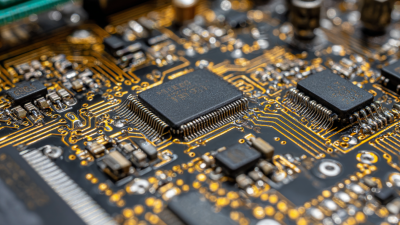
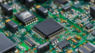
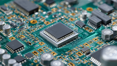
The solder mask plays a crucial role in the overall performance and reliability of printed circuit boards (PCBs). It acts as a protective layer, preventing solder bridges, minimizing the risk of short circuits, and ensuring that only designated areas are soldered. A well-applied solder mask enhances the integrity of electrical connections, significantly impacting the longevity and functionality of the PCB.
Moreover, the choice of solder mask material influences thermal performance and chemical resistance. For instance, high-temperature solder masks can withstand prolonged exposure to heat, making them ideal for applications in automotive or aerospace industries. Additionally, the color and texture of the solder mask can affect the visibility of components during assembly, thus impacting production efficiency. Overall, the effectiveness of solder masks in safeguarding PCBs underscores their importance in achieving optimal operational performance and reliability.

When working with solder masks on your DIY PCBs, understanding the application and curing process is crucial for achieving a professional finish. Solder mask helps to protect the copper traces and prevent solder from bridging between them, which is essential for optimal performance. To get started, ensure that the PCB is thoroughly cleaned before applying the solder mask; contaminants can lead to adhesion issues.
Tips: When applying solder mask, considerations should include the thickness of the mask and the type of application method you choose—whether it's spray, screen printing, or photo-printing. Each method has its pros and cons, so choose one that suits your project’s needs. Furthermore, be mindful of the curing process; proper curing ensures that the solder mask adheres correctly and can withstand the heat of soldering.
If you encounter any defects, don’t worry—there are various solder mask repair techniques available. These can range from using a solder mask repair pen to applying new solder mask material over the affected areas. It’s essential to assess the damage and choose a method that will restore functionality without compromising the overall integrity of the PCB. With these best practices, you'll enhance the durability and performance of your DIY projects.
When it comes to solder mask printed circuit boards (PCBs), various common issues can impact optimal performance. One of the prevalent problems is inadequate adhesion of the solder mask to the substrate. According to a 2021 IPC report, nearly 30% of PCB manufacturers reported issues related to solder mask delamination which can lead to solder shorts and other mounting defects. This is often caused by improper surface treatment or contamination, making it essential for manufacturers to ensure proper cleaning and preparation of the PCB surface before applying the mask.
Another frequent issue is the misalignment or design flaws in the solder mask layer. Misalignment can lead to areas of exposed copper, causing solder bridging during assembly. A study published in the Journal of Electronic Materials highlights that misalignment errors account for about 15% of soldering defects in PCBs. To mitigate these risks, it is crucial for designers to correctly align the solder mask with the pads and vias, and to utilize reliable software for accurate layout design. Implementing stringent quality checks during the production process can significantly enhance the reliability of solder mask PCBs, ensuring optimal performance in end-use applications.


„Thanks to the LUVIR technology, the solder resist process could be switched directly from the previously used mask exposure to direct exposure. As an outstanding digital solution on the market, this technology has been able to demonstrate fast process times and superior quality on our certified conventional ink in production. This allowed us to fully digitize the solder mask process at low cost – without process or ink adjustments. An excellent benefit to our production in Rot am See.“
Ralf Göhringer (Head of Production WE Rot am See)
I would definitely recommend the Limata machine and team for a future company purchase
Michael Greenaway
Compunetics Inc.
“The Limata ldi has been amazing!! Best thing we did was buy this machine”
Richard Brady
GM
Circuitlabs
“Since 2019, we have been running the Limata X1000 LDI system (including LUVIR for solder mask imaging) in daily production as an addition to our current process with film. The machine was capable of properly exposing Taiyo PSR-4000 BN (DI) solder mask types on normal to high-copper boards using a new and unique direct imaging process. The machine operating interface is very user friendly which allowed for a quick technical training curve. The pre-registration processing reduced several seconds of production time at every print. Limata support and service staff is incomparable. They supported our team every step of the way at basically any time of the day or night, with literally, an immediate response time, customizing the software interface to best fit our Operations and needs.
We have exposed more than 8,000 prints since end of October, on various solder mask colors and some resist film panels. Limata, has proven to be very capable and innovative. They are a strong contender in the industry.
We have very much enjoyed this project, and working with the team!
Thank you Limata for the continued support and being a part of our growth.”
Bill Sezate
Vice President, GM
Summit Interconnect
As a replacement to our current contact exposure process with film, the LIMATA X2000 system including LUVIR-Technology was capable of properly exposing non-LDI solder mask types using a direct imaging process. The machine offers cutting edge software with a very intuitive operating interface which allowed for quick technician training curve. The dual drawer system combined with pre-registration processing reduced several seconds of production time at every machine cycle. Limata support and service staff is world class. They added software patches to keep production running at shortest possible response times, customized the software interface to best fit our in-house Operations system, and even wrote a step-by-step machine processing manual. As a result of the project, we have exposed more than 16,000 times on various product types and solder mask brands/colors. Limata, in a very short timeframe as a company, has definitely shown they are truly innovative and will be challenging the industry of direct imaging for the top spot.
Kevin Beattie
Process Engineer
TTM Technologies
Forest Grove Division