An EV charging unit must manage power while operating in a compact enclosure, often near heat-producing components and switching circuits. Its printed circuit board is more than a platform for connecting parts. The layout influences current paths, signal quality, heat flow, and the unit’s ability to operate reliably over repeated charging sessions.
EV Charging Module PCB Design matters because small decisions can have practical consequences. A narrow copper path may warm under sustained load. Poor separation between noisy power traces and sensitive control signals can contribute to unstable readings. Connector placement also affects assembly, inspection, and service access. These details are easy to overlook on a screen. They become more obvious when a prototype runs hot or a technician struggles to reach a test point.
Good design requires choices based on the module’s electrical demands, thermal conditions, materials, and manufacturing process. Engineers may use simulation and design reviews, but measurements from prototypes remain important. A tidy schematic is not enough. Real hardware can behave differently than expected, and that gap deserves attention rather than excuses. Thermal checks, current testing, and careful review of component ratings can help reveal weaknesses before production. No single layout guarantees reliability; design constraints vary between products. Still, a disciplined PCB process gives teams a clearer way to manage risk, support consistent manufacturing, and build charging equipment that performs as intended.
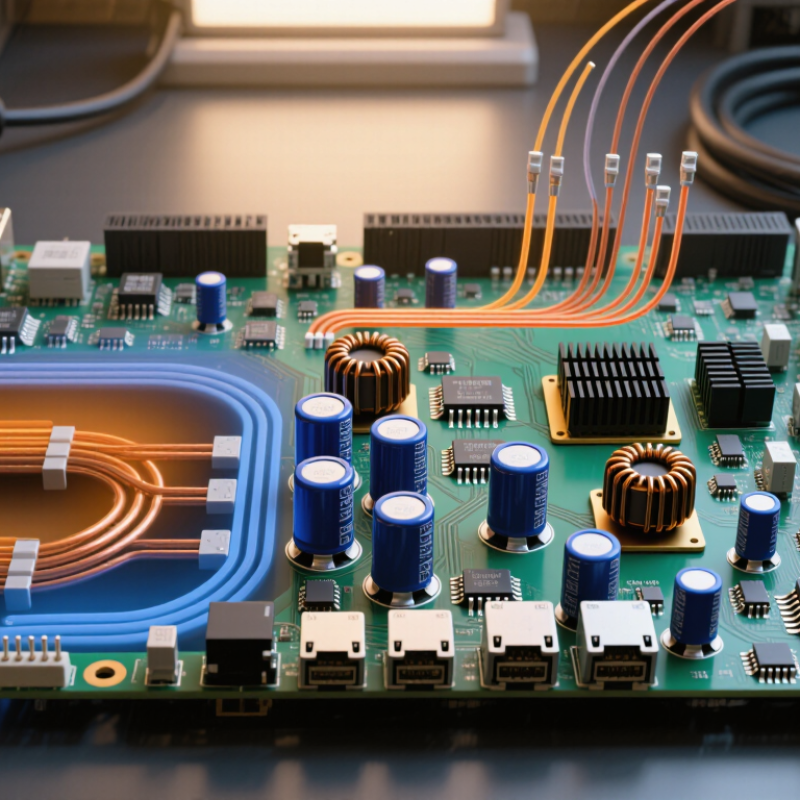
Why Is EV Charging Module PCB Design Important?
A 7–22 kW AC charger and a 350 kW DC fast charger may look similar from the outside. Inside, their demands differ sharply. AC charging usually relies on the vehicle’s onboard charger for power conversion. DC equipment performs that conversion in the charging station, placing heavier demands on power modules, control circuits, and thermal paths. At 350 kW, even small losses can become substantial heat. Heat is unforgiving.
The International Energy Agency’s Global EV Outlook 2024 reports that public fast-charging points above 22 kW grew by 55% in 2023, reaching about 1.3 million worldwide. That growth makes reliable module design practical, not theoretical. A PCB must support accurate voltage and current sensing, robust isolation, and carefully routed switching signals. Designers also need to manage electromagnetic interference and keep hot power components away from sensitive control circuits. Copper thickness matters. So does the path from component to heatsink.
Power ratings need context: a 350 kW station does not mean one PCB carries all that power. Systems commonly distribute conversion across modules, while the PCB coordinates switching, protection, and monitoring. This is where layout decisions show up in the field: a noisy sensor reading can trigger needless shutdowns, while poor thermal contact can shorten component life. I would not treat a clean schematic as proof of a dependable design. Testing under heat, load changes, and real cable conditions still matters.
AC charging commonly ranges from 7 to 22 kW, while DC fast-charging examples range from 50 to 350 kW. These are representative power ratings; actual charging speed depends on the vehicle, charger, and operating conditions.
Trace power from the grid to the vehicle, and the PCB sits at every critical handoff. In an AC charging module, incoming power passes through protection and filtering, then rectification and power-factor correction. A DC link stores energy briefly before an isolated converter adjusts voltage for the vehicle’s battery. In a DC fast-charging system, much of this conversion happens in the charger cabinet, and regulated DC travels to the vehicle. The exact path depends on the system. Heat tells a story.
The PCB must carry high current without creating excessive resistance or hot spots. Wide copper paths, suitable spacing, robust connections, and effective thermal management help keep power delivery stable. Sensors and control circuits also monitor voltage, current, and temperature, allowing the module to respond when conditions shift. A small layout weakness can become a real fault under sustained load. Still, no layout is perfect: adding copper or spacing may increase board size and cost, so engineers must balance competing needs.
Tips: Follow the power path on the schematic, then compare it with the physical board. Check connector joints and copper areas after testing at realistic loads. Small details matter. A cool-looking board at low current may behave differently during a long charging session.
At 350 kW, system voltage has a major effect on current. At 400 V, the idealized figure is about 875 A; at 800 V, it is roughly 438 A. The arithmetic is simple. The hardware is not.
At 400 V, that current demands careful power-path design, solid connections, and close thermal checks. A PCB may carry control signals and some power, while busbars or other conductors handle the heaviest loads. Ordinary traces alone are not a realistic solution. At 800 V, lower current can reduce conduction losses for the same resistance, but higher voltage brings tougher insulation and component-rating requirements. Layout still matters.
Designers need to examine copper geometry, connection resistance, heat flow, and switching noise together. A tiny hot spot near a connector can undermine an otherwise sound module. Current sensing and protection also depend on clean, reliable signal paths. And 875 A versus 438 A is a useful comparison, not a complete operating specification: actual values vary with voltage, efficiency, and load conditions. The neat calculation can hide messy details, and those details deserve bench testing.
Why Is EV Charging Module PCB Design Important?
An EV charging module PCB must carry high current while switching power quickly in a confined space. The IEA reported that public charging points grew about 40% in 2023, while fast-charger installations rose 55% (Global EV Outlook 2024). That growth makes compact, thermally robust layouts increasingly important. A few millimeters of misplaced copper can create a hot spot near a connector or power device.
Heat spreads through copper planes, component pads, and thermal vias, but it does not distribute evenly. Designers must check current density and temperature rise against the real enclosure, airflow, and duty cycle. IPC-2152 offers guidance for estimating PCB current-carrying capacity; actual prototypes still matter. Simulations can miss contact resistance or a blocked air path. That is worth remembering.
Switching noise depends on layout, not just component choice. Keep high-current switching loops short, place decoupling capacitors close to switching devices, and provide clear return paths. Small loops matter. Poor routing can create voltage overshoot, interference, and extra stress on components. Insulation needs equal care: maintain suitable spacing between high-voltage nodes and low-voltage control circuits, accounting for board material and contamination. Creepage and clearance should be checked against the applicable insulation requirements, not guessed from a neat-looking layout. A layout review should trace each current path and inspect the thermal and insulation margins.
For conductive EV charging, IEC 61851 turns safe operation into a set of electrical and control requirements. IEC 61851-1 covers general requirements for charging systems, including the control-pilot functions that help coordinate connection and charging states. The PCB must carry those signals reliably while separating low-voltage control circuits from hazardous power paths. Small errors matter. A noisy pilot trace or poorly placed isolation barrier can undermine a design that looks sound on paper.
The scale is growing. The IEA’s Global EV Outlook 2024 reports that public charging points increased by 40% in 2023, reaching about 3.3 million worldwide. That growth raises the value of robust, repeatable module design. Engineers need to consider creepage and clearance, component temperature, fault detection, and electromagnetic compatibility early—not after the first prototype warms up under load. Heat is stubborn. Copper width, thermal vias, and enclosure airflow can change how a board performs during sustained charging. Testing should also check pilot behavior across real cable and connection conditions. One uncomfortable detail: passing a bench test does not guarantee reliable field operation. Good PCB design makes IEC 61851 requirements measurable in the hardware, while leaving room for careful verification.
| PCB design dimension | Relevant IEC 61851 area | Design relevance | Typical verification evidence |
|---|---|---|---|
| Protective separation and insulation | IEC 61851-1: general requirements for conductive EV supply equipment; applicable insulation-coordination and safety requirements depend on the equipment and installation. | PCB spacing, isolation components, slots, and routing barriers help prevent hazardous voltage from reaching control, communication, or accessible circuits. Required clearances and creepage distances depend on factors such as working voltage, pollution degree, and material properties. | Insulation-coordination review, component ratings, PCB layout inspection, and applicable dielectric-strength or insulation-resistance test results. |
| Protective earthing and fault paths | IEC 61851-1 safety provisions for EV supply equipment, including protective measures relevant to the equipment configuration. | A well-planned protective-earth connection and fault-current path support reliable protection. PCB connections should not create unintended breaks, narrow bottlenecks, or reliance on signal-ground paths for protective functions. | Protective-earth continuity and bonding checks, inspection of connection points, and fault-condition testing as applicable. |
| Control-pilot interface | IEC 61851-1 defines control-pilot functions for communication and control between the EV and the EV supply equipment in applicable charging arrangements. | Input protection, filtering, accurate signal measurement, and robust grounding help the controller recognize pilot states and respond appropriately. The control-pilot circuit must be designed for the specified interface and operating conditions. | Control-pilot waveform and state measurements, tolerance analysis, and checks of charging responses under normal and fault conditions. |
| Proximity and cable-related sensing | IEC 61851-1 covers charging-system control functions; connector and cable arrangements determine which proximity-related functions apply. | Protected inputs and suitable thresholds allow the control board to interpret supported connector or cable signals. Layout should reduce noise coupling from switching power stages into low-level sensing circuits. | Input-threshold and noise-immunity checks using the applicable connector and cable configuration. |
| Charging-current switching and monitoring | IEC 61851-1 establishes general EV supply equipment requirements; IEC 61851-23 adds requirements for applicable DC EV supply equipment. | Power paths, current-sense circuits, switching controls, and thermal design must support the equipment’s declared operating range. High-current conductors and sensitive measurement traces require appropriate separation and routing. | Current-measurement calibration, temperature-rise testing, switching checks, and operation across the specified load range. |
| Overcurrent, overvoltage, and fault response | IEC 61851-1 and, for applicable DC equipment, IEC 61851-23 address safety and equipment-level requirements; protection details depend on the system design. | Protection circuits need dependable sensing, suitable component ratings, and control behavior that places the system in a safe state when specified faults occur. PCB layout can affect detection accuracy and response reliability. | Protection-threshold measurements and documented fault-injection tests for the relevant operating modes. |
| Electromagnetic compatibility and signal integrity | IEC 61851-21-2 specifies EMC requirements for off-board EV charging systems within its scope. | Grounding strategy, return paths, filtering, shielding connections, and separation of noisy and sensitive circuits influence emissions and immunity. Good PCB design helps reduce interference that could disrupt control or monitoring. | Applicable emissions and immunity test reports, plus functional checks during and after EMC testing. |
| DC charging communication interface | IEC 61851-24 addresses digital communication between a DC EV charging station and an electric vehicle for control of DC charging. | Where this communication is used, the PCB must support the selected physical interface and maintain signal quality, isolation, and noise tolerance appropriate to the system architecture. | Interface conformance checks, communication tests, and functional verification during representative charging sequences. |
| Environmental and thermal robustness | IEC 61851 equipment requirements apply alongside the environmental conditions and ratings specified for the product and installation. | Component derating, copper sizing, thermal paths, coatings where appropriate, and connector selection help the board withstand its specified temperature, humidity, and operating environment. | Thermal measurements and environmental tests selected for the declared product ratings. |
Note: IEC 61851 requirements depend on the charging mode, equipment type, installation, and applicable edition. Confirm the relevant standard clauses and test methods for the specific design; this table is a design overview, not a compliance checklist.
„Thanks to the LUVIR technology, the solder resist process could be switched directly from the previously used mask exposure to direct exposure. As an outstanding digital solution on the market, this technology has been able to demonstrate fast process times and superior quality on our certified conventional ink in production. This allowed us to fully digitize the solder mask process at low cost – without process or ink adjustments. An excellent benefit to our production in Rot am See.“
Ralf Göhringer (Head of Production WE Rot am See)
I would definitely recommend the Limata machine and team for a future company purchase
Michael Greenaway
Compunetics Inc.
“The Limata ldi has been amazing!! Best thing we did was buy this machine”
Richard Brady
GM
Circuitlabs
“Since 2019, we have been running the Limata X1000 LDI system (including LUVIR for solder mask imaging) in daily production as an addition to our current process with film. The machine was capable of properly exposing Taiyo PSR-4000 BN (DI) solder mask types on normal to high-copper boards using a new and unique direct imaging process. The machine operating interface is very user friendly which allowed for a quick technical training curve. The pre-registration processing reduced several seconds of production time at every print. Limata support and service staff is incomparable. They supported our team every step of the way at basically any time of the day or night, with literally, an immediate response time, customizing the software interface to best fit our Operations and needs.
We have exposed more than 8,000 prints since end of October, on various solder mask colors and some resist film panels. Limata, has proven to be very capable and innovative. They are a strong contender in the industry.
We have very much enjoyed this project, and working with the team!
Thank you Limata for the continued support and being a part of our growth.”
Bill Sezate
Vice President, GM
Summit Interconnect
As a replacement to our current contact exposure process with film, the LIMATA X2000 system including LUVIR-Technology was capable of properly exposing non-LDI solder mask types using a direct imaging process. The machine offers cutting edge software with a very intuitive operating interface which allowed for quick technician training curve. The dual drawer system combined with pre-registration processing reduced several seconds of production time at every machine cycle. Limata support and service staff is world class. They added software patches to keep production running at shortest possible response times, customized the software interface to best fit our in-house Operations system, and even wrote a step-by-step machine processing manual. As a result of the project, we have exposed more than 16,000 times on various product types and solder mask brands/colors. Limata, in a very short timeframe as a company, has definitely shown they are truly innovative and will be challenging the industry of direct imaging for the top spot.
Kevin Beattie
Process Engineer
TTM Technologies
Forest Grove Division