Choosing a circuit board solder mask is not a cosmetic decision. It affects insulation, solderability, trace protection, and inspection. For buyers, the right choice depends on board design, assembly process, operating conditions, and budget. Small details matter.
Prismark’s annual PCB industry reports track changes in board production, product mix, and regional demand. IPC’s electronics manufacturing surveys provide further context on production conditions and supply-chain pressures. These sources help explain why buyers should assess solder-mask options against actual manufacturing needs, not just unit price. They do not, however, establish one universally best mask. That distinction is easy to overlook.
Common options include liquid photoimageable (LPI), dry-film, and epoxy-based masks. LPI is widely used because it supports fine patterns and suits many standard PCB designs. Dry-film can be useful for specific board geometries, while epoxy systems may fit simpler applications where cost is central. The IPC-SM-840 specification provides a recognized framework for solder-mask qualification and performance. Still, a standard cannot replace a supplier’s process data or a buyer’s own design review.
This guide compares the main types by application, manufacturability, protection, and cost. Ask suppliers about minimum dam width, coating thickness, color consistency, and compatibility with your assembly process. Request evidence for the conditions your board will face. Then verify it on a sample. A datasheet alone can feel reassuring, but it may leave important questions unanswered.
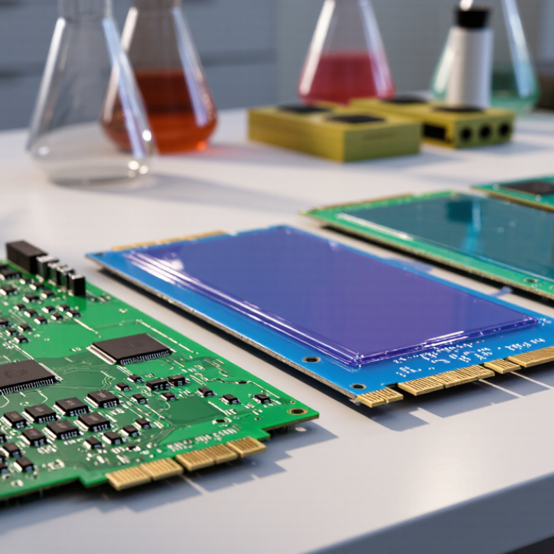
A solder mask is the thin protective layer covering most of a printed circuit board’s copper surface. It is usually a polymer coating, applied and cured after the copper circuitry is formed. Small openings are left over solder pads, connector contacts, and other areas that must remain exposed. The mask helps keep solder on those pads during assembly, reducing the chance of accidental bridges between nearby traces. It also limits copper exposure to moisture, dust, and handling.
A common process uses liquid photoimageable mask. The coating is applied, exposed through a pattern, and developed so unwanted areas are removed before final curing. This allows precise openings around fine-pitch components. Screen-printed epoxy and dry-film masks are other options, each suited to different production needs. The best choice depends on board geometry, required durability, and the assembler’s process. Tiny openings need careful alignment.
Solder mask does not make a board immune to defects. Poor registration can partly cover a pad, while an overly small opening may complicate soldering. Very narrow gaps between pads also deserve review during design, since mask dams can become fragile. Color is not a reliable quality signal; green is common, but other colors can serve the same basic purpose. That distinction is easy to miss. A buyer should check the mask material, coverage, and opening tolerances against the board’s actual use.
Solder mask is the thin polymer coating that covers most exposed copper on a printed circuit board. It helps limit oxidation, reduces accidental solder bridges during assembly, and leaves pads open for component connections. The green layer is familiar, but color is mainly a visual choice; coverage, adhesion, and registration matter more. A mask edge that creeps onto a fine-pitch pad can complicate soldering. Small detail, real consequence.
IPC-SM-840E sets qualification requirements for permanent solder masks, including tests of electrical, chemical, and thermal performance. IPC-2221B separately bases conductor spacing on voltage and conditions around the conductors. That distinction matters: mask supports protection, but it does not replace properly designed electrical clearance. Buyers should check the specified mask type, opening tolerances, and surface finish together, rather than treating “solder mask” as one universal layer.
The mask also defines the board’s visible geometry. It frames copper pads, vias, and test points, while helping keep solder where assembly needs it. A practical review should compare the Gerber openings with the actual pad layout and ask how the fabricator controls registration. I would not assume a tidy render guarantees clean openings; real boards have tolerances, and the smallest pads expose them quickly.
Solder mask forms an insulating protective layer over PCB copper while leaving selected areas exposed for soldering. This comparison shows each type’s primary pattern-defining method: photoimageable masks use photolithography, while screen-printed epoxy masks are patterned with a screen. It does not compare performance or quality.
Liquid photoimageable solder mask, or LPI, is widely used for modern circuit boards. It is applied as a liquid, then exposed through artwork and developed to open pads. This process supports fine traces and closely spaced components. A well-controlled coating also helps limit solder bridging during assembly. Cure quality matters.
Dry film solder mask is laminated onto the board as a sheet. It can provide consistent thickness and useful coverage on some board designs, but it may not suit every fine-pitch layout. Registration and lamination conditions affect the result. Small shifts can cover part of a pad.
Screen-printed, thermally cured epoxy mask is a simpler option for less demanding designs. It can be practical where cost and basic protection matter more than very precise openings. Its edges may be less sharply defined than those made with LPI. That difference is easy to overlook on a drawing. Buyers should compare mask type, opening tolerance, board geometry, and assembly needs with their fabricator. There is no universal best choice; even a familiar process can behave differently across board thicknesses and panel layouts.
Solder mask protects copper traces from oxidation, solder bridges, and handling damage. Most boards use a liquid photoimageable polymer, applied and patterned before final curing. Green remains common because it offers clear contrast for inspection, but red, blue, black, and white are also available. Color is not just cosmetic: dark masks can make fine traces harder to see, while white may show stains more readily. The exact shade can vary between production batches.
Gloss and matte describe the mask’s surface appearance, not the exposed-pad finish. Glossy coatings reflect more light; matte coatings reduce glare under inspection lamps. Neither is automatically better for every design. Also specify the copper surface finish separately, since it affects exposed pads and solderability. These choices can interact with assembly needs, lighting, and inspection methods. A small caution: color can get more attention than the practical details deserve.
Tips: Ask for the mask color, gloss level, and exposed-pad finish as separate specifications. Review a sample under your actual inspection lighting, especially for dark or white boards. Confirm that fine-pitch pads remain clearly defined. If appearance is flexible, prioritize reliable inspection and assembly over a perfect color match.
Choosing a solder mask starts with the board’s layout, not its color. Liquid photoimageable (LPI) mask is common for modern designs because it can define openings around fine-pitch pads. Screen-printed epoxy may suit simpler layouts, while dry-film options can be considered when the board’s geometry or process requires them. Ask the fabricator which materials and application methods they can control reliably. A familiar process is often safer than an unfamiliar one.
Check the smallest spacing between pads, traces, and mask openings. On a dense board, narrow mask dams can disappear or shift during fabrication. Confirm whether vias should be tented, plugged, or left exposed; each choice affects assembly and inspection. Tiny details matter. Also check the mask’s thermal and chemical resistance against the actual assembly steps, rather than relying on a general datasheet claim. Color is mostly cosmetic, but contrast can make inspection easier. One point is easy to overlook: the drawing may look precise, yet production tolerances still apply. Review the fabricator’s design rules and inspect a sample or first article when possible.



„Thanks to the LUVIR technology, the solder resist process could be switched directly from the previously used mask exposure to direct exposure. As an outstanding digital solution on the market, this technology has been able to demonstrate fast process times and superior quality on our certified conventional ink in production. This allowed us to fully digitize the solder mask process at low cost – without process or ink adjustments. An excellent benefit to our production in Rot am See.“
Ralf Göhringer (Head of Production WE Rot am See)
I would definitely recommend the Limata machine and team for a future company purchase
Michael Greenaway
Compunetics Inc.
“The Limata ldi has been amazing!! Best thing we did was buy this machine”
Richard Brady
GM
Circuitlabs
“Since 2019, we have been running the Limata X1000 LDI system (including LUVIR for solder mask imaging) in daily production as an addition to our current process with film. The machine was capable of properly exposing Taiyo PSR-4000 BN (DI) solder mask types on normal to high-copper boards using a new and unique direct imaging process. The machine operating interface is very user friendly which allowed for a quick technical training curve. The pre-registration processing reduced several seconds of production time at every print. Limata support and service staff is incomparable. They supported our team every step of the way at basically any time of the day or night, with literally, an immediate response time, customizing the software interface to best fit our Operations and needs.
We have exposed more than 8,000 prints since end of October, on various solder mask colors and some resist film panels. Limata, has proven to be very capable and innovative. They are a strong contender in the industry.
We have very much enjoyed this project, and working with the team!
Thank you Limata for the continued support and being a part of our growth.”
Bill Sezate
Vice President, GM
Summit Interconnect
As a replacement to our current contact exposure process with film, the LIMATA X2000 system including LUVIR-Technology was capable of properly exposing non-LDI solder mask types using a direct imaging process. The machine offers cutting edge software with a very intuitive operating interface which allowed for quick technician training curve. The dual drawer system combined with pre-registration processing reduced several seconds of production time at every machine cycle. Limata support and service staff is world class. They added software patches to keep production running at shortest possible response times, customized the software interface to best fit our in-house Operations system, and even wrote a step-by-step machine processing manual. As a result of the project, we have exposed more than 16,000 times on various product types and solder mask brands/colors. Limata, in a very short timeframe as a company, has definitely shown they are truly innovative and will be challenging the industry of direct imaging for the top spot.
Kevin Beattie
Process Engineer
TTM Technologies
Forest Grove Division