A printed circuit board may look finished when its copper traces are etched, but exposed conductors still face solder bridges, oxidation, and handling damage. Solder mask is the thin, patterned coating that covers selected copper while leaving pads and other connection points accessible. On a real board, that distinction appears around tightly spaced pins: a clean opening helps solder reach the pad without spreading onto its neighbor. Small detail. Significant consequences.
IPC’s IPC-SM-840 specification sets qualification and performance requirements for solder resist materials, while IPC-6012 defines performance requirements for rigid printed boards. These standards are useful professional references, but they do not promise that one mask material or process suits every design. IPC’s published North American PCB shipment and order data also shows how the industry tracks production activity; it does not provide a universal, mask-specific defect rate. That limitation matters. Claims about exact failure reductions should be tied to a particular product, process, and test method.
In manufacturing, solder mask supports electrical isolation, protects copper from environmental exposure, and helps control solder flow during assembly. Its value becomes tangible near fine-pitch components, where a misplaced opening or poor registration can expose copper or narrow the margin between adjacent pads. Color is the visible feature, but coverage, adhesion, thickness, and alignment carry the engineering burden. Mask is not magic. It cannot repair a flawed layout or careless process, and designers sometimes treat it as a final cosmetic layer. Understanding its role means examining how material selection, artwork, fabrication tolerances, and assembly conditions work together—and where their limits remain.
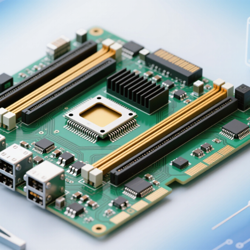
Solder mask is the thin, usually colored polymer coating on a PCB’s outer surfaces. It sits above the patterned copper and the exposed areas of the laminate, not beneath the copper. The coating follows the board’s surface, covering most copper traces while leaving designed openings for solder pads, test points, and some vias. Look closely at a bare board: the flat green field is mask; the bright metal circles are usually exposed copper finishes.
This placement matters during assembly. Mask separates neighboring copper features, helping limit accidental solder bridges and reducing exposure to moisture, dust, and handling. It is not insulation for every situation, and it cannot correct poor spacing or damaged copper. Small openings can also shift slightly during fabrication, so pad edges may show a narrow mask overlap. That detail deserves inspection, not assumption.
Prismark’s 2023 PCB Industry Report estimated global PCB production at about $73.2 billion that year and projected growth toward $90.8 billion by 2028. Those figures describe the industry, not mask performance, but they underline how widely this protective layer is used. Its color can make boards recognizable; its position and registration are what engineers need to verify. A mask is easy to overlook. It shouldn’t be.
Solder mask application begins after the copper pattern is etched and inspected. The board is cleaned to remove dust, oil, and processing residue. Even a small fingerprint can interfere with adhesion. A liquid photoimageable coating is then applied, often by screen printing or spraying. It covers the copper traces while leaving pads to be exposed later. The wet layer needs an even thickness; pooling near fine-pitch pads can cause problems. It looks simple, but it is not very forgiving.
The coated panel is partially dried, then aligned with a film or digital imaging pattern. Ultraviolet light hardens selected areas, while the image protects the openings for pads and test points. During development, uncured mask washes away from those openings. Operators check that edges are clean and copper is not accidentally covered. The mask is then fully cured with controlled heat, helping it resist soldering temperatures and routine handling. Some lines use different coating or imaging methods, so settings depend on the board design and material. A tiny registration shift can matter. It deserves a second look.
Solder mask is the thin protective coating that covers most copper traces on a PCB. It leaves component pads exposed for soldering and separates nearby conductive areas. That gap matters. During reflow, solder melts and flows toward exposed metal. Masked surfaces are less likely to collect solder, helping reduce the chance of a bridge between closely spaced pads.
The mask lowers risk, but it cannot correct every design or manufacturing problem. If pads are too close, the coating is poorly registered, or excess solder is applied, a short can still form. It is easy to treat the mask as a cosmetic layer; that assumption deserves a second look. A small shift near a fine-pitch component can change the clearance between exposed pads. Technicians can inspect these areas under magnification for thin mask edges, gaps, or solder connecting adjacent pins. The coating’s thickness and alignment also need to suit the board layout. Solder mask is useful protection, not a guarantee, and that distinction can be overlooked when a board looks clean at first glance.
During PCB fabrication, etched copper traces can be left exposed to air, handling, and soldering heat. A cured solder mask forms a protective layer over most of the board, while leaving pads and other connection points uncovered. That boundary matters. It limits direct contact between copper and moisture, dust, and residue that may contribute to corrosion over time. It also helps prevent solder from spreading across narrow gaps between adjacent traces. A stray solder bead can cause a short circuit.
The protection depends on sound coverage and adhesion. If the mask is scratched, poorly cured, or missing near a trace, moisture and contaminants may reach the copper. A small gap matters. The mask does not make a board waterproof, and it cannot repair copper that was already damaged during fabrication. In practical inspection, technicians check for pinholes, lifting edges, and uneven openings around pads, especially on densely routed boards. Clean handling and suitable storage still matter after assembly. Solder mask is a useful barrier, not an excuse to ignore the rest of the process.
Solder mask supports PCB assembly by separating copper features that should remain electrically isolated. During reflow, it helps limit solder from spreading across narrow gaps and forming bridges. The openings expose only the pads needed for components, giving solder paste a defined landing area. Small details matter. If mask registration shifts, it can partly cover a pad or leave copper exposed near a fine-pitch component. That can complicate placement and inspection.
After assembly, the cured coating shields much of the copper from moisture, dust, and handling damage. It also adds a barrier against incidental contact between conductive debris and traces. The protection is useful, but not absolute; mask cannot compensate for poor cleaning, unsuitable board design, or harsh operating conditions. It is easy to overstate its role. Long-term reliability also depends on coating adhesion, thickness, and correct clearance around pads and test points. A board may look well covered and still have weak spots at edges, vias, or damaged areas, so process checks remain important.


„Thanks to the LUVIR technology, the solder resist process could be switched directly from the previously used mask exposure to direct exposure. As an outstanding digital solution on the market, this technology has been able to demonstrate fast process times and superior quality on our certified conventional ink in production. This allowed us to fully digitize the solder mask process at low cost – without process or ink adjustments. An excellent benefit to our production in Rot am See.“
Ralf Göhringer (Head of Production WE Rot am See)
I would definitely recommend the Limata machine and team for a future company purchase
Michael Greenaway
Compunetics Inc.
“The Limata ldi has been amazing!! Best thing we did was buy this machine”
Richard Brady
GM
Circuitlabs
“Since 2019, we have been running the Limata X1000 LDI system (including LUVIR for solder mask imaging) in daily production as an addition to our current process with film. The machine was capable of properly exposing Taiyo PSR-4000 BN (DI) solder mask types on normal to high-copper boards using a new and unique direct imaging process. The machine operating interface is very user friendly which allowed for a quick technical training curve. The pre-registration processing reduced several seconds of production time at every print. Limata support and service staff is incomparable. They supported our team every step of the way at basically any time of the day or night, with literally, an immediate response time, customizing the software interface to best fit our Operations and needs.
We have exposed more than 8,000 prints since end of October, on various solder mask colors and some resist film panels. Limata, has proven to be very capable and innovative. They are a strong contender in the industry.
We have very much enjoyed this project, and working with the team!
Thank you Limata for the continued support and being a part of our growth.”
Bill Sezate
Vice President, GM
Summit Interconnect
As a replacement to our current contact exposure process with film, the LIMATA X2000 system including LUVIR-Technology was capable of properly exposing non-LDI solder mask types using a direct imaging process. The machine offers cutting edge software with a very intuitive operating interface which allowed for quick technician training curve. The dual drawer system combined with pre-registration processing reduced several seconds of production time at every machine cycle. Limata support and service staff is world class. They added software patches to keep production running at shortest possible response times, customized the software interface to best fit our in-house Operations system, and even wrote a step-by-step machine processing manual. As a result of the project, we have exposed more than 16,000 times on various product types and solder mask brands/colors. Limata, in a very short timeframe as a company, has definitely shown they are truly innovative and will be challenging the industry of direct imaging for the top spot.
Kevin Beattie
Process Engineer
TTM Technologies
Forest Grove Division